
The possibility to transfer electric power by means of electromagnetic waves was proved for the first time by Nikola Tesla, in 1890: he probably could not imagine how the discovery would have been appreciated nowadays. Standard Qi and wireless charge are terms that overwhelmingly entered the consumer sector, and in particular as for the one of smartphones and tablets, with always more models having a wireless charger for the internal battery.
Since we consider this topic an important one, we decided to launch a contest (contest.open-electronics.org), in partnership with Integrated Device Technology, Inc. (IDT®) and Würth Elektronik: what you need to do is use the kit that we will present in this post (and that you will receive FREE) for the creation of wireless power applications and you can hack with us and participate!
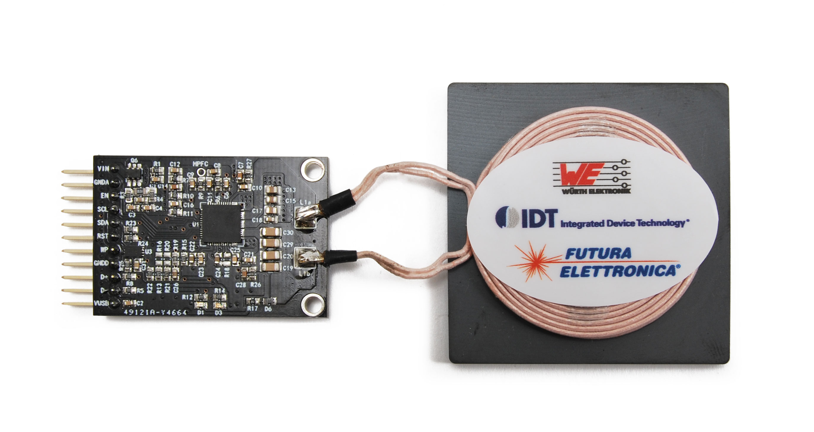
The development platform with which you will work, and that consists in two units – a transmitter and a receiver – so to let you learn their basic features before starting the development. The transmitter is the unit that irradiates the electromagnetic field, whose energy will be transferred to the receiving device placed within the operating range, and according to the modes and performances that depend on the factors that we will examine later.

THE TECHNOLOGY
Transferring energy by means of the electromagnetic waves is easy, but the real challenge is the one to make this technology more efficient and less bulky (specially for powers that are greater than the paltry ones available in the past). A challenge that becomes more difficult if we have to create cheap and miniaturized solutions, to be introduced even in the smaller devices.
In the last years, many firms have developed some devices that are suitable for the operations with this technology; among these pioneers, IDT (Integrated Device Technology) stands out, and its products have now been made available to us.
IDT is a leader in wireless power transmitter and receiver solutions for wireless charger applications, addressing all major standards and technologies with an extensive portfolio of standards-certified products. IDT has proven expertise in both magnetic induction and magnetic resonance technologies, and actively participates in the Wireless Power Consortium (WPC) and AirFuel Alliance as a board member. IDT has introduced a number of innovative and award-winning products, including the first true single-chip transmitter, the highest-output-power single chip receiver, and the first dual-mode receiver IC compatible with both WPC and PMA (now AirFuel Alliance) standards. Prominent industry players have recognized this leadership and partnered with IDT as their silicon vendor for next-generation wireless power solutions.
The here described wireless charging system uses IDT devices, and is not a veritable application, but something that is useful in order to make you familiarize with this technology; the californian manufacturer supplies also a demo kit (EVK-TX, EVK-RX) for which the full documentation is available (including the circuit diagram and the source files used in order to create the PCBs, and it is composed of a transmitter and a receiver that are capable – when coupled – to transfer a power of 5W at 5V with an available current that is therefore equal to 1A, in accordance to the WPC standard, as per version 1.1.2 of the Qi specifications).
Our project is a re-release of it, but in a miniaturized form and with circuits that are supplied with pin-strips, so that you may integrate them in your projects.
The project was born in order to supply a quick prototyping platform that would be useful for the development of your applications.
Now, let’s analyze the two units in detail; the transmitter is based on the P9038 integrated circuit by IDT, and the receiver on the P9025AC, still by IDT.
THE TRANSMITTER
The said unit, that is based on the P9038 integrated circuit, generates an alternating signal that is amplified and that goes to drive an inductor whose task is to irradiate the electromagnetic field; the amplifier stage is of the bridge type, so to allow to drive the coil by means of an alternating component, which otherwise would be impossible when working with a single power supply (as in our case). Obviously that is not all, since the integrated circuit is capable of detecting the presence of a load, a coil, in proximity of which some energy is drawn. Let’s have a look at the circuit diagram and see how the transmitter works. To stay on topic, it is possible to power the circuit from the Vin and GND contacts, the corresponding voltage must have a value between 4.5 and 6.9 Vcc.
The system may be set to standby mode – even if it still remains powered – in order to decrease the energy consumption during the stages in which it is not needed to transfer power in wireless mode: the EN (Enable) terminal has been designated for this task; it is active at a low level, therefore in the case in which it is not needed to set the integrated circuit to standby mode, it is possible to connect it to the ground (in the PCB it is connected to a 47 kΩ pull-down resistor). In the said mode the device absorbs only 600 microampere.

As said before, it is possible to choose between two power sources, and the U1 integrated circuit deals alone with managing them: if the board is powered by the pin 15 (Vbus) receives 5 V and commands the pin 47 (Gate) so that it polarizes the Q1 MOSFET’s gate, in order to make it conduct current towards the Vin line, to which the input pin of the internal regulator (REGIN) is connected; the latter supplies voltage (typically 5 V) to the rest of the integrated circuit. The line is filtered by the capacitors C22 and C23, that are useful, whichever is the circuit’s power source. Please notice the C1 capacitor, that allows the soft start of the regulator (it allows to gradually polarize the MOSFET’s gate), and the R1 resistor, that discharges the said capacitor when the GATE pin returns to the open state.
The integrated circuit also has an internal Low Drop Out (LDO) linear voltage regulator available, whose input is connected to REGIN and whose output is placed at the LDO5V pin, filtered by a 1 µF capacitor. Another low drop out linear voltage regulator is integrated in the chip, it supplies 2.5V to the LDO2P5V (20) pin.
The RS pin is used in order to reset the system and is kept at a low level by a 47 kΩ pull-down resistor; as with the ENABLE function, even for the RESET one a pad is available: thanks to the latter, it is possible to reset the transmitter, should it be the case. The only other integrated circuit that is external to the P9038 and that is used in the transmitter module is the EEPROM 24AA64T, inside of it a “standard” firmware is memorized (it is configured so to optimally operate with the suggested layout and coil); the firmware is automatically loaded each time at the system start, and the communication is carried out via I²C BUS. The EEPROM’s “WP” (Write Pulse) pin may be accessed from the outside, by means of the pad with the same name.
As for the stage that generates the signal that drives the coil, the frequency is internally set by the firmware; the bridge’s outputs are placed at the SW1A, SW1_B, SW1_C, SW1_D pins (all are in parallel and connected to the L1a terminal) on a side and at the SW2_A, SW2_B, SW2_C and SW2_D pins (in parallel among them, and connected to the L1b terminal) for the other one. C10 and C21 capacitors deal with reversing the bootstrap signal and start the oscillator. L1 is the irradiating coil, coupled by means of four parallel capacitors,operating the uncoupling in direct current and determining the resonance frequency. The alternating voltage found between L1b and ground is rectified by the D2 diode and brought – by means of the R17/R1 voltage divider – to the ends of the C16 capacitor, that supplies an almost direct voltage; the variations of such a voltage through the capacitor – due to the load – are read by the GPIO1 pin and by the ISNS, that is the input of the circuit for the demodulation and decoding of the wireless communication. GPIO1 is used as retroaction, so to optimize the functioning of the data decoding circuit. The signal that is reversed to the HPF pin is filtered by the low-pass cell that is composed of C9 and C8; HPF is the input of the signal for the demodulator.

In each half of the output bridge that drives the irradiating coil, a protection has been implemented: it limits the current on the positive branch, to the values that are defined by the components that are connected to the INSPIN and INSNIN pins, that are the inputs of the differential error amplifier (respectively, the non-inverting and the inverting one).
For the purpose of reducing the EMIs (that are unavoidable in a device of this kind), the rise and fall times of the pulses that power the coil are modulated, in a way to generate the lowest harmonic voltage possible; in fact the integrated circuit implements a system that is fit to limit the amount of the input current during the transient interferences and, along with a proprietary system for the control of the slew rate, it allows the eliminate the need for EMI filters.
The energy transfer from the P9038 to a WPC-compatible receiving device (such as, for example, the P9025AC that is mounted on our receiving unit) is managed by the latter, thanks to a data link that takes advantage of the armature reaction that takes place in the coil, because of the absorption variations that are determined by the receiver when it communicates. The data packets are overlapped to the irradiated electromagnetic field and are demodulated by the specific block in the P9038. In the case you wanted more details concerning the related protocol, please visit the official WPC website.
The A/D converter participates to the data demodulation, the microcontroller uses it in order to monitor the variations in the absorption (Foreign Object Detection), the working voltages and the associated currents, in addition to the signals incoming on ISNS.
In addition to these specifications – that have an essentially “electric” nature – IDT also took care of ensuring the security of the communication between TX and RX, by means of a 64 BIT encryption.
The input voltage and current are sampled by the ADC and processed by the firmware for the detection of external objects (FOD), according to WPC 1.1.2. As for the pins ISNS_AVG and VSNS_AVG, they have been designed for the filtering of the signals derived from the detection of the input current and voltage, respectively.
The input signal for the current detection is generated in a differential manner by the pins ISNSP_IN and ISNSN_IN. This input for the current detection is filtered by an internal 50 kohm resistor, combined with an external capacitor on the ISNS_AVG pin.
The measures of the input voltage are filtered by a 33 kohm internal output resistor on the VSNS_AVG pin, combined with an external capacitor on the VSNS_AVG pin. We recommend to keep the values that have been indicated in our diagram unchanged, so to ensure the alignment of the measures and an accurate calculation of the power for the FOD and other purposes.
The TX module is powered by means of voltages between 4.5 and 6.9 Vcc, so that it may be powered at 5 V by a standard power source but that is capable of supplying 2A. Once the connection has been established, a green LED placed on the transmitter will start to flash, so to indicate that the correct coupling with the receiver has been established. Actually, the LEDs found on the board are two: in addition to the green one we already saw, there is a red one.
This table describes the operating state of the system, on the basis of the visual indications given by the pair of LEDs:

THE TRANSMITTER BOM
| R1: 10 Mohm (0603)
R2: 0,01 ohm (0805) R3: 22 ohm (0603) R4: 22 ohm (0603) R5: 33 ohm (0603) R6: 10 Mohm (0603) R7: 47 kohm (0603) R8: 33 ohm (0603) R9: 10 kohm (0603) R10: 10 kohm (0603) R11: 15 kohm (0603) R12: 4,7 kohm (0603) R13: 4,7 kohm (0603) R14: 4,7 kohm (0603) R15: 4,7 kohm (0603) R16: – R17: 1,5 kohm (0603) R18: – R19: 10 kohm (0603) R20: – R21: 47 kohm (0603) R22: 47 kohm (0603) R23: 4,7 kohm (0603) R24: 4,7 kohm (0603) R25: 10 kohm (0603) R26: 0 ohm (0603) R27: 0 ohm (0603) R28: 4,7 kohm (0603) C1: 6,8 nF (0603) C2: 6,8 nF (0603) C3: 6,8 nF (0603) C4: 6,8 nF (0603) |
C5: 100 nF (0603)
C6: 1 nF (0603) C7: 22 nF (0603) C8: 1 nF (0603) C9: 3,3 nF (0603) C10: 1 nF (0603) C11: 6,8 nF(0603) C12: 3,3 nF (0603) C13: 10 µF (0805) C14: 22 nF (0603) C15: 10 µF (0805) C16: 3,3 nF (0603) C17: 10 µF (0805) C18: 100 nF (0603) C19: 100 nF (1206) C20: 100 nF (1206) C21: 100 nF (0603) C22: 1 µF (0603) C23: 100 nF (0603) C24: 1 µF (0603) C25: 6,8 nF (0603) C26: 1 µF 0603) C27: 100 nF (0603) C28: 22 nF (0603) C29: 100 nF (1206) C30: 100 nF (1206) D1: LED red (0603) D2: CDSU400B D3: LED green (0603) Q1: FDC8878 L1: Coil Wireless Power (PN 760308111) U1: P9038 U2: 24AA64T-I/MNY |
THE RECEIVER

Let’s move on now to the receiver, that is coupled to TX by means of the specific receiving coil: it must be said that the Qi specifications require a distance between 1.75 and 2.5 mm between the transmitter’s coils and the ones of the receiver. In order to respect the said specification and to optimize the electrical efficiency of the power transfer we inserted a small transparent plexiglass separator, glued to the big wire planar inductor, the figure shows the trend of the efficiency, with a distance of 3.7 mm, when varying the power supplied by the receiver.

The receiving unit is much simpler than the transmitting one and even the integrated circuit is smaller, because it has instead to limit itself to receive the voltage induced at the ends of the receiving coil (that is connected between the board’s contacts L1a and L1b), to rectify it in order to extract its data and to acquire the current needed for powering both the chip and the load (the power is made available between the Vrec pin and ground, GND), and to communicate by sending its own data (under the form of peaks of the absorption from the coil itself, they are obtained by shortcircuiting the latter with a MOSFET array, that is placed before the rectifier).
Let’s analyze the circuit diagram, still keeping an eye on the block diagram of the P9025AC integrated circuit, as shown in figure.

The input circuit, that is to say the one that detects the electromagnetic field, depends on the coil that – according to the electromagnetic laws – supplies a voltage whose width depends on the magnetic flux that is determined by the irradiating coil, by the angle of the axes of the two coils, in addition to the distance; as explained before, when coupling the coils this distance is the maximum possible one and therefore the power to be drawn is the maximum one as well.
The voltage at the ends of the receiving coil has an almost square wavelength (the fronts are rather dull) and flows through the resonance capacitors, C4, C5 and C6, so to reach pins 6 and 30, that are the inputs of the alternating current and that depend on a special Graetz bridge (rectifier), that is implemented by four diodes. Each one of them is placed between drain and source of as many n-channel MOSFETs, that are in turn commanded on the gate by the signals supplied by the Driver & Control block. The latter is synchronized, by means of the voltages received on the bootstrap pins BST1 and BST, thanks to the C10 and C8 capacitors, with a voltage supplied by the coil, so to achieve the maximum efficiency. The voltage, being so rectified, is applied to the Vrect pin and to the ground (GND) ones and is periodically sampled, thanks to the internal ADC, that is assigned to various functions – via a multiplexer – by the control logic. The latter reads the corresponding digital value and possibly acts on the control unit of the MOSFETs, so to set the regulation curve. If the voltage on Vrect, as levelled by the C11÷C16 capacitors, goes under the internally set threshold value (as a result of the load), the logic sends a request to the transmitter, for the purpose of lowering the frequency, so to reach the resonance one as much as possible (a condition in which, as taught by Electrical Engineering, the current is the maximum one; here we are talking about a RLC series dipole, as is the corresponding circuit at the transmitter’s output and at the receiver’s input). On the other hand, if the voltage on Vrect tends to grow too much, the transmitted data tell the transmitter to increase the frequency, so to exit that resonance range.
In order to increase the efficiency as much as possible, the voltage on Vrect is kept as much as possible close to the output one of the internal LDO regulator block (that powers all the logic stages and the ADC), especially if the load at the output of the same LDO grows. At low loads, a high Vrect is set, so to better face sudden load increases.
The regulation of the Vrect is obtained by means of the four MOSFETs, each one connected in parallel to one of the diodes of the Graetz bridge: as the load grows, each one of them starts to conduct for a period ranging between the beginning and the end of the concerned half-wave, thus supplying additional charging current of the capacitors to the Vrect output. The Driver & Control block deals with synchronizing the conduction of the MOSFETs, it grasps the incoming pulses from the coil and synchronizes the pulses sent to the gates with them; the control is a sort of PWM: the more the current needed, the greater the width of each pulse, and vice versa.
When the mobile device containing the P9025AC is placed within the electromagnetic field created by the transmitter, it answers the transmitter’s “ping” signal (query) by rectifying the alternating current and by memorizing it on a capacitor that is connected to the VRECT. During the “ping”, the rectifier supplies about 5V to the VRECT pin. An internal linear voltage regulator supplies the power voltage to the digital section, so to allow the WPC communication. The P9025AC then communicates its univocal ID and the configuration information to the transmitter. After this, the system enters the power transfer mode. The P9025AC’s regulation circuit then regulates the voltage of the 7V rectifier, by sending the Control Error Packets instruction to the transmitter. The LDO output is activated and the power is supplied to the load, after that VRECT reaches 7V.
When power is supplied to the load, the P9025AC control circuit continues to send control error packets to the transmitter, for the purpose of regulating the rectifier’s voltage to the required level, so to maximize the efficiency of the linear regulator.
The transmission towards the transmitter is carried out by taking advantage of the principle of the armature reaction, by opportunely loading – by means of the MOSFETs connected to the ACM1, ACM2, CLMP1 and CLMP2 pins – the dipole composed of the L1 receiving coil and of the C4, C5, C6 capacitors; since the group of the two coils, is in all respects an air-core transformer, the load on L1 results in a request to increase the magnetic flux that is determined by the transmitter’s coil, and therefore in an increase of the transmitter’s absorption, that is detected by the P9038’s internal logic.

The P9025AC’s I²C bus is connected to contacts SDA, SCL (referred to GND) and each one of the corresponding pins is supplied of a pull-up resistor that is connected on the high side to the I2CR external line, that must be brought to the microcontroller’s power source. You might possibly want to interface the latter to the receiver. For the purpose, the U1’s SCL and SDA lines are of the open-collector type.
Even the receiver’s chip supports the advanced detection of the external objects (FOD), which is needed in order to identify the loss of efficiency that is caused by the introduction – inside of the operating range – of electrically conductive items. During the energy transfer, the receiver periodically communicates the received amount of power to the transmitter, by means of a data packet named Received Power packet. The transmitter compares the value contained in it with the amount of power that is transmitted during the same period of time. If there is a significant loss of power, the transmitter stops supplying power to the coil, since a possible unrelated object could absorb so much energy to cause overheating.
In order to have a WPC system to carry out this function with sufficient accuracy, both the transmitter and the receiver must calculate and compensate their known losses.
Such losses could be resistive losses, that are determined by metal parts in the surroundings, and that are part of the transmitter or of the receiver, etc. Since the system accurately measures its power and knows all the intrinsic losses, it is possible to detect the unrelated objects, by detecting further losses that are due to them.
The P9025AC uses advanced FOD techniques and accurately compensates all the known losses. This compensation is carried out by means of a fitting curves table, that supports up to 10 different curves that are memorized in the OTP (One Time Programmabile) memory. The 10 programmed settings are externally chosen by means of the value of the resistance connected to the FOD1 pin and read by the ADC, under the form of a voltage drop to its ends. Moreover, the I²C-Bus interface supports the FOD compensation setting, that may be selected and that is overwritten on the OTP memory. The following table shows the values taken by the resistance, in correspondance of 10 expected values: from 1 to 10 the efficiency of the energy transfer increases. A further improvement of the compensation is obtained by also using the FOD2 pin, whose resistance determines a ±300 mW offset on the value that have been selected by the FOD1 resistor. This is useful in order to tune the compensation curve, by optimally selecting upwards or downwards, in line with well known current losses of the receiving system.

Even the receiving chip has an enable pin (pin 14, /EN), when set to low level it enables the activity, while at logic 1 it sets the component to standby mode; we returned it to the expansion pin-strip.
The pin 15, TEOP (supplied of an internal pull-down resistor), is particularly interesting, when set to high level it it disables the internal LDO and sends a WPC End-of-Power message with a 0x03 code (over-temperature) to the transmitter, thus stopping the transmission. It may be used, in combination with a temperature sensor that is applied to the battery, in order to stop the charging if it heats too much (which is very useful with lithium batteries, that explode when overheated).
On the other hand, the pin 32 (/STAT) indicates that the charge is in progress and goes to logic zero in such a condition; it may be used in order to communicate to a microcontroller that we are nearing a charging station.
THE RECEIVER BOM
| R1: 4,7 kohm (0603)
R2: 4,7 kohm (0603) R3: 0 ohm (0603) R4: – R5: 47 kohm (0603) R6: 30 kohm (0603) R7: 4,7 kohm (0603) C1: 470 nF (0603) C2: 22 nF (0603) C3: 1,8 nF (0603) C4: 47 nF (0603) C5: 100 nF (0603) C6: 100 nF (0603) C7: 1 µF (0603) |
C8: 10 nF (0603)
C9: 22 nF (0603) C10: 10 nF (0603) C11: 100 nF (0603) C12: 470 nF (0603) C13: 4,7 µF (0603) C14: 4,7 µF (0603) C15: 4,7 µF (0603) C16: 4,7 µF (0603) C17: 1 µF (0603) C18: 4,7 µF (0603) D1: LED Green (0603) L1: Coil Wireless Power (PN 760308111) U1: P9025AC-RNBGI |
PRACTICAL IMPLEMENTATION
It is convenient to enclose the transmitter’s coil within two 3 mm thick plexiglass slates, so to have an already calibrated distance when you place the receiving device. Actually, if you mount the transmitter in a container acting as a base for the device to be recharged, please consider the thickness of the partition to which you will apply the receiver’s coil, and as a consequence you may be able to do without the plexiglass on the irradiating coil. It is understood that no metal barrier (nor one in electrically conductive plastic) must be inserted between the transmitting and the receiving coils, otherwise you will verify a strong loss of efficiency or even the impossibility to make the system work.
In order to ensure a 5.3V output voltage with a maximum current of 1A available for the user connected to the receiver, IDT advices to power the transmitter with a power source capable of supplying 5V with a maximum current of 2A. Once the wireless connection has been established, the green LED on the receiver’s PCB will be turned on, so to indicate that the power transfer is correctly taking place, and that there is 5.3V between the OUT and GND terminals. Since the LED is an optional, it might not be mounted; anyway its absorption (1mA) is really a very low one for a system that is capable of supplying 5W, therefore we would advice to keep it, at least for the purpose of having an indication concerning the system status, especially during the stages of testing and development of your application.
During the tests we carried out in the lab, the system transferred 5W, therefore ensuring an 5V output voltage of the receiver, with a 1A current.
Among the possible applications for the system, there is the one concerning the recharge of sealed gear having a battery that is an internal one, or that cannot be removed or that doesn’t have accessible contacts (as an example, a sealed car tracker that may not be recharged with the connections); since the receiving device may detect the electromagnetic field created by the transmitter (by communicating it from pin 32), it is possible to couple it to a mower or vacuum cleaner robot, that is automatically recharged when it reaches the home station.
What is your vision? Drop it in the Contest and you can receive a Wireless Power Kit for FREE and if you make it, you could Win fantastic prizes.
THE WIRELESS POWER CONTEST

Show us your ideas on how you want to use the Wireless Power kit developed by Futura Elettronica.
The Wireless Power kit includes a FT1235 5W transmitter 5W and a FT1236 5W receiver.
Joining this cordless contest is easy:
- Step 1: Register in our site
- Step 2: Submit your Wireless Power idea, win 1 of 100 Wireless Power kits
- Step 3: Build and submit your project with Wireless Power kit and WIN
Discover how to partecipate and the fantastic prize in the Wireless Power Contest page.

THE SPONSORS
IDT
Integrated Device Technology, Inc. develops system-level solutions that optimize its customers’ applications. IDT’s market-leading products in RF, timing, wireless power transfer, serial switching, interfaces, automotive ASICs, battery management ICs, sensor signal conditioner ICs and environmental sensors are among the company’s broad array of complete mixed-signal solutions for the communications, computing, consumer, automotive and industrial segments. Headquartered in San Jose, Calif., IDT has design, manufacturing, sales facilities and distribution partners throughout the world. IDT stock is traded on the NASDAQ Global Select Stock Market® under the symbol “IDTI.”
Additional information about IDT can be found at www.IDT.com.
Follow IDT on Facebook, LinkedIn, Twitter, YouTube and Google+.
Würth Elektronik
Würth Elektronik eiSos is one of Europe’s biggest manufacturer of electronic & electromechanical components. More than 550 sales representatives worldwide make up a direct sales network that is unique in this industry: Local Design in support, all catalogue products in stock and samples free of charge is the promise to our customers. Würth Elektronik operates production plants in Europe, America and Asia. More than you expect!
Additional information about Würth Elektronik can be found at www.we-online.com.
Follow Würth Elektronik on Facebook, LinkedIn, Twitter and YouTube.
Futura Group
Futura Group srl is one of the few Italian companies working in electronics field. Characterized by making disclosure and teaching through own magazine, own books and own web portals, promoting new technologies and new components.
Futura Group is known from the foreign world with the Blog Open-Electronics.org. Born in 2011, this web site presents and promotes the projects developed by the Futura Group’s team in Open Source key, also it features interviews and news. Immediately appreciated by the makers of all the world, this blog is among the most followed of the open-source field.
Additional information about Open-Electronics.org can be found at Open-Electronics.org.
Follow Open-Electronics.org on Facebook, Google+, Twitter and YouTube.

[…] Discover all the features of the Wireless Power Kit on our blog […]
[…] that have become the hallmark of the Company’s wireless power kits. It’s very close to the Wireless Power kit used for our Power […]