- Building a 3D Digital Clock with ArduinoPosted 4 months ago
- Creating a controller for Minecraft with realistic body movements using ArduinoPosted 5 months ago
- Snowflake with ArduinoPosted 5 months ago
- Holographic Christmas TreePosted 5 months ago
- Segstick: Build Your Own Self-Balancing Vehicle in Just 2 Days with ArduinoPosted 6 months ago
- ZSWatch: An Open-Source Smartwatch Project Based on the Zephyr Operating SystemPosted 7 months ago
- What is IoT and which devices to usePosted 7 months ago
- Maker Faire Rome Unveils Thrilling “Padel Smash Future” Pavilion for Sports EnthusiastsPosted 7 months ago
- Make your curtains smartPosted 8 months ago
- Configuring an ESP8266 for Battery PowerPosted 8 months ago
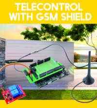
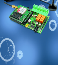
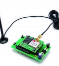
GSM Remote Control – 2 IN and 2 OUT
Part 2 – Schematic
In order to understand the different functions, let’s now take a look at the schematic diagram of the unit.

2 IN and 2 OUT Schematic Diagram
The entire control is handled by a Microchip PIC18F46K20-I/PT microcontroller, programmed with a firmware that controls the GSM/GPRS module’s activity, reads the logic condition of the two opto-isolated inputs and sends commands to the two relays in the device. Having said that, let’s take a better look at the electrical scheme: power is supplied by continuous voltage, not always stabilized (applied to PWR, + and -) at a value between 5 and 32 V; such voltage is filtered at the bottom by the diode protecting against polarity inversion (D1) through condensers C1 and C2. Fuse F1 enables you to protect both the circuit and the power source in case of short circuit in the integrated regulator discussed below, which is necessary to obtain the 3.6 V, needed for the rest of the circuit to work. The switching regulator U1 is based on a MC34063 chip, used in the classic configuration of the PWM regulators series, charged by inductance, whose output voltage depends on the energy stored in L1; the regulator is stabilized by the component demoted from resistive divider R2/R3, which is needed to set the output tension at 3.6 V. The impulses produced by the inducer’s switching are then leveled by condensers C4 and C5. The 3.6 volts at the bottom of the above mentioned condensers are then filtered by other condensers placed on the power lines of the microcontroller and of the GSM module; which presents, during transmission, absorption peaks compensated for by C7, C8, C13, C14, C15 and C16, thus avoiding that an impulsive current request may cause the microcontroller to be disturbed. The PIC is used in the configuration with an internal clock oscillator; both the scheme and the printed circuit are nevertheless equipped with external quartz, intended for those who want to modify the firmware and develop applications requiring an external oscillator. Once the I/O lines have been initialized, the microcontroller verifies the logical state of the opto-isolated inputs at voltage level (RB4 and RB5) as well as that of lines RC4, RC5, RD0, RD3, RX, which are needed to receive the main notifications from the cellular module; more specifically, RD3 is used to detect incoming calls (it interfaces with RI of the cellular module), while RC4 controls the GSM “field LED”, whose output (dubbed LED) pulses at a frequency of 1 Hz when the module is searching for the radio-mobile network, and supplies impulses at logical zero, lasting 0.5 seconds, followed by a 2-second pause, when the module has grasped the signal. The frequency and duration of the impulses enable the PIC to understand the conditions of the radio-mobile network range and to behave accordingly; for example, if the opto-isolated input goes off and therefore needs to send SMS or make calls, but detects that the cellular module has no reception, it waits for the module to get reconnected to the GSM/GPRS network before making any calls. The microcontroller contains a UART accessible via pins 44 (transmission) and 1 (reception) which it uses in order to communicate with the mobile; more precisely, through the first pin (TX), it cyclically questions the module to check whether any SMS has been received, whereas both TX and RX are used for the communication between the microcontroller and the GSM module when making calls and receiving or sending messages. Regarding the UART, the following control signals are used: CTS (Clear To Send), RTS (Request To Send) and DCD (Data Carrier Detect), which correspond to those of the cellular module being used.
Lines RC5 and RD0 complete the set of I/Os destined to the mobile; the former controls the turning on and off of the GSM (through a transistor placed in the small board of the mobile), the latter takes care of resetting the mobile. The button for locally handling this device’s operating mode is read through line RA3, set as input and equipped with an external pull-up resistor (R11), therefore active at a low level. Inputs are read through lines RB4 and RB5, both of which are set as input and equipped with an internal pull-up; each of them reads the state of the output transistor of the corresponding optocouplers (the optos used here are TLP181). Each of the two available inputs (IN1 and IN2) is active when under voltage between 3 and 30 V. When a 3-volt voltage (at a minimum) is applied to input IN1, the optocoupler’s LED is switched on and the output phototransistor is in conduction state; therefore, the collector (pin 5) is at about zero volt during the I/O initialization, due to the fall on the resistor of the internal pull-up that was configured. If the input is not polarized, the opto-isolator gets inhibited and its pin 4 is at a high level. As for the relays, they are controlled by the microcontroller’s RC0 and RE2 lines, through two NPN transistors driven by current amplifiers; line RE2 controls transistor T1, while line RC0 controls transistor T2.
A high logical state causes the transistor to saturate, thus determining the mount of current flowing in the coil of the corresponding relay. Each instance of activation is signaled with a LED, powered along with the coil. In order to protect the transistors’ collector junction as it goes from saturation to inhibition, when the relay’s coil inductance generates peaks of inverse voltage, we have connected a diode parallel to the coil, such diode eliminates unwanted impulses. The full exchange is made available from the relays so as to allow for the handling of circuits requiring a normally closed contact or a normally open one. Still regarding the relay, we should note that, although it is a 5-volt-coil type, it works on just 4 volts in our circuit; this is possible because the model we have chosen can prompt relay exchange even at less than 3.5 volts.
The PIC is programmed in-circuit, through the ICSP connector, which is attached to lines /MCLR, PGU and PGC; the microcontroller’s power and mass are also connected to the ICSP. But we didn’t think that was enough, so we included a serial communication interface enabling users to program the data related to the various functions (e.g., list of phone numbers, handling of input levels, text of SMS sent by the circuit following commands, etc.) through a PC: this allows users to program their remote control before activating it, thus avoiding having to send configuration SMS, which can anyway be used at any time, but are best used only once the system has been installed in situ.
Since the UART is already busy communicating with the cellular module, serial communication occurs via lines RE0 and RA5, respectively used as TX and RX; AN3, assigned to the internal A/D converter, is needed to detect the presence of the 5 volts and therefore the connector insertion.
The serial interface is at a TTL level and can easily be connected to a USB converter USB such as FT232 by FTDI, in order to interface the microcontroller with a PC equipped with USB. For the interface, you can use the FT782M, a small module produced by Futura Elettronica (www.futurashop.it), already equipped with a pin-strip connector at a pitch of 0.10 inches (2,54 mm) that can be directly inserted in our circuit, on the TTL connector, a female SIL at a pitch of 0.10 inches (2,54 mm).
Still regarding the device’s configuration, it is important to note that the corresponding data is not saved in the microcontroller’s EEPROM, but in an external memory chip, dubbed 24FC256-SN; it is a 256- kbit EEPROM CMOS with serial access, and with an I²C-Bus interface. In order to communicate with such chip, the microcontroller initializes its I/O lines RD4 and RD5, used, respectively, as SDA (data line) and (clock line).
Moving the remote control’s configuration data into an external memory allows us to take advantage of the entire internal EEPROM to enhance its available functions.

Related Posts


-
 Arduino ISP (In System Programming) and stand-alone circuits
We use an Arduino to program other ATmega without...
- Posted 12 years ago
-
-
-
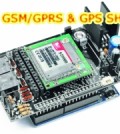 GSM GPS shield for Arduino
Shield for Arduino designed and based on the module...
- Posted 12 years ago
-
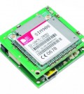
 Small Breakout for SIM900 GSM Module
Some post ago we presented a PCB to mount...
- Posted 13 years ago
-
 Join Maker Faire Rome 2024: Innovation Unleashed at Gazometro Ostiense | Calls Now Open!
All Calls Now Open for Maker Faire Rome 2024...
- Posted 2 weeks ago
-
 Building a 3D Digital Clock with Arduino
Project to create a digital clock consisting...
- Posted 4 months ago
-
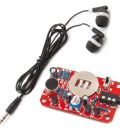 Acoustic amplifier – in DIY Kit
This kit creates a microphone amplifier with an output...
- Posted 5 months ago
-
 Creating a controller for Minecraft with realistic body movements using Arduino
Project of a controller that maps body movements...
- Posted 5 months ago
-