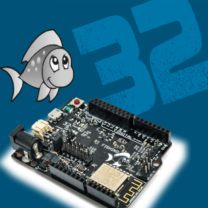
Our prototyping board acquires a 32-bit processor and sets the bar high, towards demanding applications that may take full advantage of the WiFi support, of the RTC and of the SD-Card, that make Fishino stand out from the common Arduino UNO. First installment.
Almost a year ago we presented Fishino UNO, an Arduino-compatible board, that was born for enabling access to the Internet and to the IoT world, without need for dedicated shields. The favourable reception encouraged us to create two further units, powered by a rechargeable battery, so that they may be used when missing the network power: Fishino Mega, for those who need more pins and memory for their applications, and Fishino Guppy, the smallest “fish” in our fish tank, for the truly miniaturized applications.
What else could we add? When looking around and developing, we realized that the limitations imposed by the 8 bit processors – the Atmega 328p and the Atmega 2560 – started to be felt, both in terms of space for the applications, and in terms of performances.
We, therefore, decided (since a while already, to be honest, but the effort from both the hardware and the software aspects required long development times) to move on to a 32-bit processor. Alright, but which one?
It has been difficult to choose from what is available on the market.
For reasons that we will soon explain, we went a bit against the tide, thus leaving the Atmel processors (and therefore the ARM) in favor of Microchip’s PICs (in the 32-bit version, MIPS architecture).
Our original choice was the “brand new” MCU PIC32MZ, the most performing series, but at a later time, because of the immaturity of the hardware and, above all, given that actually a truly open source USB stack is actually missing, we fell back on the well tested PIC32MX series that, in addition to not suffering from any of the abovesaid problems, has the advantage of being somehow less expensive, which is not unimportant.
That’s a relatively second-best, given that the model we used has some remarkable performances, that is to say a 120 MHz clock, a 528 kByte Flash Memory and a 128 kByte RAM memory: that’s a huge difference in comparison with what we were used with the 8-bit models, and it opens new and interesting possibilities!
Since we took the “great leap” in the 32-bit world, we asked ourselves if it was possible to add something else to our “ancestor” board, that is something we already imagined as for our well-tested and much loved Fishino UNO format. The PIC processor has an incorporated (native) USB interface, which is something that makes us save the space that would have been devoted to a converter; moreover we decided to suppress the external RTC, given that the controller we used has an internal one, that is supplied with many additional possibilities, in comparison with the DS1307 that has been used in Fishino UNO; as an example, it has the capability of waking up the controller from the standby mode at preset times and intervals.
How to use the additional space, then? As a first thing, we inserted the well-tested SEPIC power supply, that is found in the Mega and in the Guppy boards already, thus making it possible to power it via battery. What else could we add? Well, a nice audio codec!
The codec we chose is the very well-tested ALC5631Q, whose complete features we will list in the dedicated section; for the moment, it will suffice to say that it includes a stereo DAC (digital/analog converter), a stereo ADC (analog/digital converter), a class D amplifier, capable of directly driving a couple of speakers, microphone inputs, an equalizer, audio effects such as pseudo-stereo and spatial stereo… and much more. With this component it is possible, for example, to create (and without need for additional hardware) an audio player, a voice feedback for your projects (wouldn’t it be nice, as an example, if our Fishino could read out the temperature of a probe?), an audio recorder, a voice control, etc. It is even possible to take advantage of the codec for the purpose of creating a polyphonic synthesizer, which is something that will be of interest for the music enthusiasts.
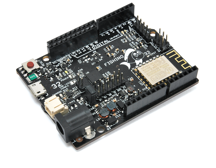
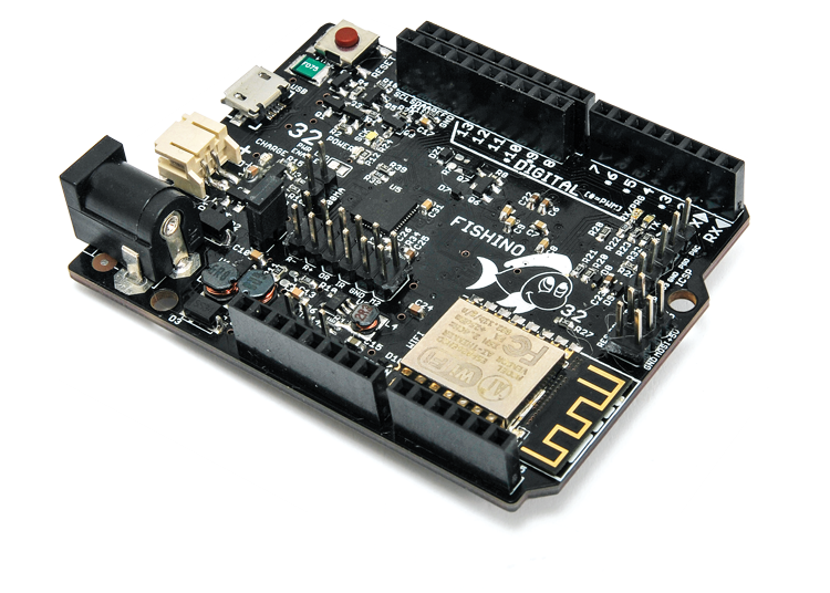
Therefore, here are the features for our Fishino 32, the progenitor of a 32-bit series whose second model is already ready (it has inferior features but an extremely small size. We will present it soon):
- PIC32MX470F512 processor;
- 512 kB ROM;
- 128 kB RAM;
- 120 MHz clock;
- native USB interface, both for the Device and the Host;
- built-in RTC;
- microSD cards supported;
- WiFi module;
- audio codec;
- powered via battery, plug and/or USB connector, from 3 volts and up to 20 volts;
- automatically recharges a LiPo battery, if an external power source is found;
- it is possible to turn off the whole board via software, leaving only the processor in standby mode;
- it is possible to wake it from the standby mode by means of an external pin or at preset times, via RTC;
- Arduino UNO standard format;
- internally operates at 3.3 volts;
- 5V-tolerant digital pins, therefore there is no risk to burn the board with a 5 volt shield.
Moreover, we added a “treat”: thanks to an expressly designed bootloader, it is no longer needed to have any external connection in order to update the WiFi module’s firmware; by pressing and holding the reset button, the board will be automatically prepared in the update mode, by taking advantage of the USB connector.
Someone will probably be worried by the difficulty of programming this new board, but we feel to reassure him; thanks to the work of the Arduino team, that made the IDE an “extensible” one in an extremely easy way, thanks to the work of the Chipkit team (of which we took advantage, even if with many modifications), thanks to the good amount of software libraries that we wrote and/or adapted, the board is programmed exactly like a common Arduino UNO, by means of the IDE and with the syntax we are used to.
It is enough to execute a small procedure while in the IDE itself, that enables the activation of the development tools for the MCU PIC, and it’s taken care of. As for the additional components, we prepared a series of libraries that will enable to take full advantage of them; some of them (and above all, the audio library) are in the development stage, and therefore they will be frequently updated.
Was this enough to stimulate your maker appetite? Let’s move on to the examination of the circuit diagram.
Circuit diagram
Let’s start from the power supply stage, that proves to be certainly more complex, in comparison with the previous models, and for the following reasons:
- the need to operate both as a host and as a USB device;
- the triple power source;
- the possibility to turn off the whole power supply stage via software;
- the possibility to only activate the power source for the controller in standby mode.
Let’s start from the control section of the USB power source; this section must be capable of supplying power to Fishino from the USB connector (if connected as a device), while it has to supply adequate power to a device that is possibly connected to Fishino (in the latter case, it behaves as a USB host).
In order to be able to execute the commutation, the pin that refers to the USBID line comes in handy, the latter is connected both to the USB connector and to the specific controller port.
The small microUSB cables are made so to have a pin at an end that corresponds to the USBID connected to ground (type A), while at the other end the pin is disconnected (type B); the device to which the type A end is connected takes on the initial role of host and, at the same time, it supplies power to the other device (this one being connected to the type B end) that takes on the initial role of device.
We talked about initial roles for a specific reason: in an OTG connection, the two connected devices may change their role; the specification only guarantees that the line will always be powered by the device connected to the A end.
Let’s return, therefore, to our diagram; we may see that the USBID line is connected to a high value resistor (R2, 100 kohm) towards ground, whose purpose is only the one to not let the line fluctuate in the case the power is missing, and a resistor, R4, whose value is certainly lower (10 kohm), that is connected between the two sources of the Q4 and Q5 MOSFETs. As it may be inferred from the diagram, a positive voltage (5V minus the direct drop on the diodes) is always found in these sources (thanks to the diodes that are internal to the MOSFETs); it comes either from the USB port or from the 5V power from the Fishino board. We are therefore certain that R4 is connected to the +5V pin under any operating condition. If the USBID line is disconnected from ground (type B connection), this positive voltage – by means of R4 – brings the n-channel Q3 MOSFET to conduction, that in turn brings the p-channel MOSFET Q1 to conduction; at the same time (and still by means of R4), the two previously seen MOSFET, Q4 and Q5, are brought to interdiction and, since they are connected in antiseries, they do not enable the power to pass from Fishino’s 5Vs to the USB connector.
In summary, with a fluctuating USBID (therefore when we insert a type B connector), Fishino does NOT supply power to the USB connector that, on the other hand, supplies power to Fishino by means of the Q1 MOSFET. We, therefore, obtained the first part of the desired objective, that is to say, that by means of a type B connector, Fishino obtains the power from the USB line, by acting as a veritable device.

If – on the other hand – we insert a type A connector, the USBID line is placed to ground, which brings Q4 and Q5 to conduction at the same time (and still by means of Q3) while Q1 is brought to interdiction; the power flows therefore from Fishino to the USB connector and does not re-enter “from the back door” since Q1 is interdicted.
Obviously, it must be noticed that in the second case (type A connection), in order to supply 5V to the USB port, Fishino must be powered in some other way, that is to say via the battery or the VIN plug, as we will see later.
When going on towards the lower part of the circuit, we notice the series of the diodes, D1+D4 and D2+D3, respectively the first ones are for the low currents, while the second ones are the power diodes. Moreover, we may see the Q2 MOSFET, to which the power from the battery comes.
Even here, the functioning is quite a subtle one; the power diodes (D2 and D3), along with the Q1 MOSFET, form an OR power port, that goes into the circuit’s VOR line. The functioning of the diodes is quite a simple one: the greater voltage between the ones of VIN and VUSB is transmitted to VOR, while the other one is isolated, because of the interdiction of the corresponding diode. One could wonder why we didn’t simply insert a power diode on the battery line, as for the other two, which would have actually made the circuit simpler, with the creation of an OR power port with three diodes. This can be done, but there is the usual problem of the voltage drop on the diodes that, while it is practically negligible for high voltages, for low voltages such as the one of the battery it brings considerable losses: intuitively, it is possible to say that a voltage drop of 0.5 volt out of 10 volt corresponds to 5%, while a 0.5 volt drop out of 3.6 volt is equal to about 14%, which is reflected on the current absorption, as we will see later, and right where a greater efficiency would be needed, that is to say as for the battery power.
The Q2 MOSFET does not have this problem, since it does not have a constant voltage drop as diodes do, but has a thermal resistance, and a particularly low one as regards the selected model; on the other hand, a MOSFET does not have the advantage of the diode that conducts only when needed, therefore a system is needed in order to bring it to conduction or to interdict it, according to the needs. That’s why we use two diodes for the low currents, D1 and D4; the functioning of the whole is as follows:
- if no power is found on VIN and not even through VUSB, the R3 resistor brings Q1’s gate to ground, the latter therefore conducts and enables the battery’s voltage to flow towards VOR;
- if on the other hand one of the two is found (VIN or VUSB, or both), one of the two diodes, D1 and D4, starts to conduct and positively polarizes Q2 that goes to interdiction, thus disconnecting the battery.
Briefly, if we have an external power source, that comes from the VIN plug or from the USB connector, the battery is disconnected; if on the other hand, the external power source is missing, the battery becomes operational.
It may be noticed that the line on which the diodes D1 and D4 go into has a name – BATOFF – since this signal, that is at a high level if an external power source is found, will be used in another circuit’s section as well.
Let’s see now the group of components that refer to the Q6 and Q7 MOSFETs; they are needed in order to disconnect the +3V3 line (that is to say the main line at +3.3V) from the +3V3Core line, that is destined to power the controller only. What are they used for? They are used in order to simply avoid that the power destined to the controller only (that is activated when all the rest is turned off, and that has the purpose of keeping the internal RTC and other minimal functions active), flows into circuits that we want to keep turned off.
Normally, if a voltage is found on the +3.3V, it goes through the diode that is internal to Q6, and even through the same Q6 if it is not in conduction, to the controller’s +3V3Core power; this is the normal functioning. If on the other hand we take away the power from the 3.3V, and at the same time we bring the OFF line to a low level, by means of Q7 we bring Q6 to interdiction and therefore we prevent the +3V3Core to go power the rest of the board. The OFF line is commanded via controller, as we will see later, during the scheduled shutdown.
It is then possible to notice the lithium maintenance battery, G1, and the D6 diode, that are used in order to supply voltage to the controller when all the other sources capable of powering it are missing. For such a reason we need to pay attention: if we completely take away power from Fishino, this battery will end up powering the whole board, unless we “take action” by means of the software, and bringing the OFF line to low level. Therefore, and unlike the 8-bit boards (in which the battery was needed only for the maintenance voltage for the RTC, and that was automatically managed), here a support intervention of the software is needed, otherwise the battery would be drained in a few minutes. We, therefore, advise to not use it and to leave the maintenance to the LiPo battery, unless you know how to manage the board’s energy saving via software.
Lastly, we notice the PWRGOOD line, that is connected via a voltage divider to ground; this supplies a positive signal to a controller’s I/O that indicates the presence of adequate power on the board, and that may be indeed used in order to manage a situation in which the power is missing, and for the standby functions. As said before, it is a quite complex management, for which a dedicated library is being prepared; as for the moment, unless you know how to manage it, we advise not to use the software shutdown functions.
The last part of the section now being examined is the one that revolves around the U1 linear regulator, that is a common low voltage regulator (maximum of about 100 mA) and a very low-power one, and that is destined to supply the maintenance voltage to the controller via the external LiPo battery. This has the same effect of the G1 lithium battery, but with the undeniable advantage of using a rechargeable battery, capable of supplying an extremely long autonomy, even with an energy usage that is not a negligible one.
This section may be deactivated by cutting the BCK jumper, that is normally connected. Even here, the remarks we made before, on the subject of the energy consumption, are valid ones (even if in a less pressing way): if we turn off the board via software, the controller will draw power from the LiPo battery, that will, therefore, tend to run out; it is a task of the software to place it in standby mode or anyway in one of the available low energy usage modes.
Let’s move on now to the switching stage section, that refers to the U2 integrated circuit (SX1308), a step-up asynchronous converter (that is used here in SEPIC mode), that is capable of supplying 5V as an output, with input voltages that may vary from about 3 to over 20 volts, and that refers to the U3 integrated circuit, that is a step-down synchronous converter, that is used in order to obtain 3.3 volts for powering the most of the circuit.
Both these stages have already been widely described as for the Fishino Mega and Guppy boards and, as regards the functioning of the SEPIC, it has been described when dealing with the Torpedo board, that was published here. The only differences lie in the presence of the ON jumper, that enables to insert a switch button that is capable of taking away power from the whole board (with the exception of the maintenance power that was possibly enabled, as explained in the previous paragraph), and in the OFF line that (as seen before) – if brought to ground – is capable of turning off the switching converter.
This line is under the processor’s direct control by means of an I/O, and therefore enables both the complete switching off of the board via software, and the isolation of the power section of the controller only from the rest of the circuit, as seen in the previous point.
In summary, by placing an OFF line to ground, all the power is taken away from the board; obviously, this line must be kept to ground by the controller, that therefore must remain operational by means of one of the two maintenance power sources (LiPo or lithium battery); if those are missing, by bringing the OFF line to ground we would only obtain a board reset and a consequent reboot of the whole.

As regards the battery charger, it refers to the ever-present MCP73831, a complete integrated single cell LiPo charge regulator; that’s the same one found in Fishino Mega, therefore as for the details we refer you to the related article. The only notable point is given by the Q9 n-channel MOSFET, that is used to enable the battery charging function.
If we remember the first stage’s description (power control), the BATOFF line is at a high level when an external power source is found; in this case the Q9 MOSFET goes in conduction, by bringing the R15 resistor to ground (and possibly the R16 if we selected the charging at 500 mA), thus activating the charging. When external voltages are missing (battery power) the BATOFF line goes to low level, thus deactivating the charging.
Please notice the R17 and R18 resistors, that form a voltage divider that is capable of supplying half of the voltage of the LiPo battery, that can be measured by means of a controller line so to signal the charging state of the same. We used a voltage divider since the LiPo battery’s voltage when fully charged, exceeds 3.3 V that are accepted by the controller’s analog inputs; when measuring it is therefore needed to take them into account.
Controller stage
We have finally reached the PIC32MX470F512, for the time being we will just examine some of its connections only, and leave the rest to the other stages, as for the details. As a first thing we may notice two quartzes, a 20 MHz one and a 32,768 kHz one; they are needed since the first one supplies the main clock, by means of an internal PLL, that multiplies it up to 120 MHz. That is not really a low-power circuit, therefore it is to be avoided in conditions requiring to save power; on the other hand, the 32,768 kHz quartz is exclusively needed for the real time controller (RTC) that is internal to the PIC, that is a circuit that has been specifically designed for to have a very low absorption and that therefore may be left working even in standby mode.
Let’s return to the first quartz: if we accepted a lesser accuracy on the frequency, it could have been removed; in fact, the PIC has an internal RC oscillator that is quite an accurate one, and it is capable of almost getting the job done. We said “almost”, since the internal oscillator has two flaws:
- it is not as accurate as the quartz (this has a relative importance);
- it is not capable of bringing the PIC to its maximum frequency of 120 MHz, because of restrictions of the internal PLL, and therefore it would be limited to 96 MHz.
The first point is only important if we use the board for accurate measurements of short times, as an example as a frequency or period meter; as for long times the other quartz should be enough.
The second point is a binding one, if we want to push the controller to its limits, and therefore we added it!
Please notice – among the different connections on the controller – the three ones we saw before, that is to say the OFF one, that enables the possibility to take away the main power, the PWRGOOD, that enables to control the state of the same, and the MBAT line that enables the measurement of the battery voltage.
Let’s take a look now at the reset section, that is an interesting one since it enabled us to use only a single reset button for different functions, in combination with a specific bootloader on the controller. We immediately notice three lines that refer to the reset stage:
- MCLR;
- REMOTERESET;
- LONGRESET.
The MCLR line is the veritable reset one as for the controller; by bringing it to ground it is rebooted.
We immediately notice that this may occur both by pressing the reset button that – by means of the C22 capacitor – sends a short negative pulse to the MCLR line, and by bringing the REMOTERESET line, that comes from the WiFi module, to ground, that therefore enables the latter to reset the controller.
The LONGRESET line, on the other hand, is found to ground for the whole time in which the reset button is being pressed, thus enabling the bootloader to know our intentions.
In brief:
- by shortly pressing the reset button (under 2 seconds) or by means of a negative signal on the REMOTERESET line, the board will be rebooted, as usual;
- by keeping the reset button pressed for a time interval between 2 and 4 seconds, the bootloader will be started (which is something that is highlighted by the orange LED flashing), thus placing the board in the sketch loading mode;
- by keeping the button pressed for more than 4 seconds, the firmware upgrade procedure as for the WiFi module will be started, as highlighted by the blue LED flashing.
It is, however, possible, once we have entered the 2 bootloader’s modes, to simply restart the board and to execute the preloaded sketch by shortly pressing the reset button again.
As regards the LED section, it simply includes two LEDs that are connected to as many controller ports, that may be used for whichever task (they are respectively indicated on the board as RX/PRG and TX) and the usual LED that is connected to port 13, that is used in the board tests (BLINK program), and this occurs via the Q9 MOSFET, so to not load the D13 exit, and by the way, that reflects the SPI interface’s clock line (SCK) state, that is something that you may notice when using a microSD card or a WiFi module.
Let’s move on now to the WiFi section, that is similar to the one in the previous Fishino boards, since the module still has a firmware we created, that is capable of high speed communication, via the SPI port and not via the serial one.
We eliminated the ESPCONN connector from this board; we got used to it on the previous boards and some I/Os and control pins of the module referred to it and were used both to program it and – as for some of them – were used as additional I/Os.
The reason for this lies in the fact that in Fishino32 we already have freed some I/Os that were used in order to communicate with the module and with the SD card, and they were number 4, 7 and 10; we also divided the I²C bus from the two analog inputs, A4 and A5, thus obtaining 3 additional digital ports and 2 additional analog ports that are now available.
In addition to that, two ports on the ICSP connector may not be used as additional digital ports (we will talk in detail about that when describing the software), therefore we preferred to take advantage of the connections with the ESP module in another way. In fact, all the ESP lines (with the exception of the analog input) are now under the control of the main processor, which enables us to carry out the following operations directly, via software, without having to keep any I/O busy:
- to reset the module via software;
- to turn off the module via software (which previously required the usage of a Fishino’s I/O);
- to load the firmware on the module, without having to carry out any weird connection or to load any particular sketch;
- to redirect the module’s serial output on the USB serial or on any other serial – both software and hardware – that is available on Fishino.
As for the rest, nothing changes with respect to the previous boards; the communication is carried out via the SPI port, that refers to the SD card and to the digital pins, D11, D12 and D13, on the external connector.
Given that the PIC we used has two incorporated SPI interfaces, one would wonder why one of them was not dedicated to the included modules (the WiFi and SD ones), thus freeing completely the 11, 12 and 13 I/Os as well; we did it like this since the second SPI interface is dedicated – in I²S mode, to the audio codec to which it is fully committed, when the latter is operating. At first, we had chosen that path, but we later realized that it would have been impossible, as an example, to play an audio file read by the SD card, since during the reproduction the interface was totally busy with the codec, without having the possibility to access the SD card. It must be said that as for the boards in the Arduino UNO format, the 3 above said I/Os are anyway dedicated to the SPI port, and anyway if needed we have the 2 aforesaid I/Os on the ICSP port available, and possibly all the analog I/Os that may anyway be even used as for the digital. The interface towards the microSD is identical to the one in the previously seen boards; it takes advantage of the SPI interface, as the WiFi module does, while even here as for the selection of the board an internal I/O is used, thus freeing the D4 I/O that was previously needed for the purpose. The only big difference with respect to the previous boards is that the level converter stages (from 5 to 3.3 V) are missing, since the PIC uses 3.3 V as power, thus making a direct (and faster) connection possible. There is only a precaution to take into account, when executing existing sketches: the board selection pin (CS) is no longer the 4 (or 10 as in some Arduino versions) but an internal pin named SDCS; it is therefore enough to substitute all the references to the I/O 4 with I/O SDCS (to be written just like this, since it may physically change from board to board).
Audio Codec Stage
And here we are with the juicy innovation concerning Fishino32: the audio codec! It is based on the ALC5631Q chip, which is used in many consumer products (tablets, audio player, etc.) and therefore it is capable of very remarkable performances, while still maintaining a more than acceptable price. The codec has the following features:
- a 24-bit D/A (DAC) stereo converter, having a signal-to-noise ratio of 100 dbA and a total distortion of -90 dB;
- a 24-bit A/D (ADC) stereo converter, having a signal-to-noise ratio of 93 dbA and a total distortion of -88 dB;
- a class-D stereo amplifier, capable of supplying 650 mW per channel, if powered by 3.3 V on a 8 Ohm impedance, and up to 2.8 W per channel if powered (as in our case) at 5 volts and on a 4 Ohm impedance;
- an amplifier for stereo headphones, capable of supplying 45 mW on 16 Ohm, that, unfortunately, we won’t use on our board, because of space limitations;
- 3 analog differential inputs or an analog stereo input (we will use the latter);
- two analog preamplified microphone inputs, both in the differential (the one we used) and in the single-ended mode;
- a stereo digital microphone input (even this one has not been used on our board, still because of space limitations);
- an analog line input, to which it is possible to connect an external amplifier;
- a complete power management system, that enables to turn off the individual codec components, if they have not been used;
- a 6-band audio digital equalizer;
- pseudo-stereo and spatial stereo effects;
- noise removal circuits as for the noises found when the speakers are turned on and off;
- automatic level control (ALC) both for the reproduction and the recording;
- standard high-speed I²S interface (24 bit/from 8 and up to 192 kHz on the DAC when reproducing and 24 bit/from 8 and up to 96 kHz on the ADC when recording).
As it may be noticed, this is a series of impressive features, that will enable the creation – without the need for any additional hardware, exception made for a speaker or a microphone – of many projects that involve the digital audio; as an example:
- audio players (as for WAV and MP3);
- audio recording;
- vocal recognition;
- music synthesizer
- voice synthesizer
As you will see soon, we already implemented a .wav files player, and a complete MP3 reader is in the works; software libraries for recording and other features will be released soon.
As we hinted when talking about the WiFi module, the codec takes advantage of a dedicated SPI interface, that is used in the I²S mode, and in order to manage it we wrote a specific software library.
Moreover, the codec needs an I2C port (it must not necessarily be a dedicated one, and in fact we used the standard Fishino I2C port) in order to control all the various available functions. Here we created a specific library that is capable of controlling the codec functioning; by means of it, it is possible, as an example, to decide whether to record or reproduce, to modify the audio volume, to regulate the equalizer, to set the ALC, etc.
As you may easily imagine, there is a lot of commands, therefore the libraries will be gradually extended, as soon as the need arises.
There is very little to add to the circuit diagram; as you may see, aside from the codec, there are some uncoupling capacitors on the power sources and the I/Os, a capacitor for an internal converter that is destined to increase the voltage for the headphones amplifier (C38) and a couple of resistors for the bias voltage (polarization) of the microphones. There is not much else to be said!
Talking about the I2S interface: this is an interface that is based on the SPI and that has been expressly designed for the transmission of high-speed stereo audio streams; differently to the SPI, and because of the fact that the signals that transit on it must be real time ones, it is impossible to use it, in practice, on various devices at the same time.
The interface uses the usual SDI (MISO), SDO (MOSI) and SCK (clock) pins for the data, while the selection pin is used in a different way in order to select the audio channel (between the two that have been transmitted); moreover an additional clock one is used as a reference.
Therefore we have, by naming the pins from the master side, that is to say, from the controller’s point of view:
- MISO or SDI > ADCDAT, that is to say, the input data from the A/D converter to the controller;
- MOSI or SDO > DACDAT,
that is to say the output data, from the D/A converter towards the PIC; - SCK > BLCK, that is to say the clock for the single bits sent;
- SS > LRCK, that is the clock in order to differentiate the left and the right channel;
- MCLK > Reference Clock, usually four times the SCK.
The transiting signals may be seen in the figure , in which the reference clock (MCLK) is missing, it is anyway a fixed quadruple-frequency clock, with respect to the BLCK.

For the time being, we will stop with the codec description, and we will consider it again when talking about the software libraries.
Expansion Connectors
In this section all the connectors bringing signals to the outside of the board are grouped: therefore there are the side headers, the ISP connector (that has not been used in order to program the board, on Fishino32, but it has been inserted for reasons of compatibility with the existing shields), the ICSP connector (In Circuit Serial Programming) that is used in order to program the board without having to go through the bootloader (as an example, in order to program the bootloader itself), and on which two additional digitals I/Os are available, and the USB connector.
As hinted before (when talking about the board’s features), the PIC has many tolerant I/O 5 V pins (but not all of the I/O pins are 5 V tolerant) , that is to say, they are capable of accepting 5V as an input, without being damaged, even if the controller is powered at 3.3 V. Whenever possible, we took advantage of those pins by bringing them to the outside as digital I/Os; unfortunately, in some cases this has not been possible and we had, therefore, to insert an input protection by means of resistors and diodes; this is the case of the signals on the SPI port (the I/Os going from 11 to 13) that, being necessary to the internal modules as well, we should have limited anyway.
The protection consists of a 220 Ohm resistor in series at the input, and in a diode that is capable of discharging the excess on the 3.3 V line, thus limiting the input voltage to such a value.
On the analog pins – that are not 5V tolerant ones – (right because of the analog circuitry that is internal to the controller) we inserted only some resistors in series, in order to limit a possible overcurrent in the case in which some values above 3.3 V were inserted.
Please pay attention, as this does not mean that it is possible to add 5 volts on that connector! The resistors offer a minimal degree of protection, that should protect the controller for short times if – as a mistake – 5 volts are inserted, but you should not take them into account and durably use them with such voltage values!
In fact, the integrated circuit is internally supplied with protection diodes, they act as those we added externally on the inputs D11 to D13; however these diodes are only capable of absorbing a very limited current and for short periods of time, therefore you should absolutely not lean on them.
In the header section you will also find a connector named REFSEL, that is used in order to select the voltage that will be connected to the VREF pin; it is, in fact, possible to make the 5V come here, in the case in which “normal” shields (that operate at the said voltage) are used, or the 3.3 V that are destined to low voltage shields such as the ones used in Arduino DUE.
From openstore

[…] A 32-BIT FISHINO board for your powerful IoT!Posted 4 weeks ago […]