Having explained the theory, let’s see in practice the project of the SEPIC power supply.
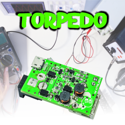
In this post we discussed – on a theoretical level (even if in a simplified way) – the SEPIC switching converters, also highlighting advantages and disadvantages, and giving you the basics for the calculation of their components. Let’s get to the heart of the project, now; we will present a practical application of the previously explained concepts: a power supply that we named Torpedo. It is a switched-mode power supply with a SEPIC configuration, that was born in order to execute some tests finalized to substitute – when we were developing our Fishino UNO board – the underperforming linear regulator that was found in it, and in all Arduino boards. The features that we wanted were:
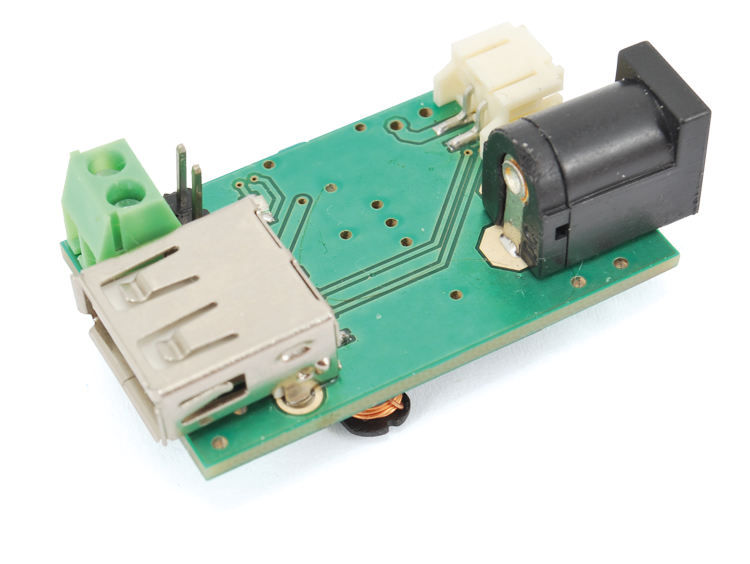
- triple power source, that is to say: the USB, the battery and an external one;
- wide range of values as for the input voltage: from 3 to 20 volts;
- minimum output current of 500 mA, with the possibility to reach 1A and more, via an external source;
- high efficiency, above 70% and possibly above 80-90%;
- single-cell LiPo battery charger incorporated;
- a transition from battery power to another source that is without interruptions;
- 5 V output with high stability, having a low ripple and when varying the load.
As we will see later, all the project specifications have been respected in Torpedo.
Circuit Diagram
In order to better understand our circuit’s functioning, we may divide the diagram in three blocks:
- input stage;
- battery charger;
- SEPIC converter.

The input stage is composed mainly of the D5 and D6 diodes, that coupled with the Q1 MOSFET form the power source selector.
We will momentarily neglect the Q1 MOSFET and deal only with the D5 and D6 diodes and with the protection diode that is internal to the MOSFET itself: the three voltages – coming from an equal number of inputs, BAT, USBIN and PS1 – directly polarize the three diodes and therefore tend to make them start to conduct, reaching up to U2’s VIN pin. Clearly, the greatest voltage among the three of them brings the diode to conduct and causes the interdiction of the other two, that turn out to be inversely polarized; this system is actually an OR power port, that is to say, it carries out the selection by bringing the highest voltage (among the three available ones) to VIN. The diodes prevent that the highest voltage goes to an input having a lower voltage.
The above said diodes (D5, D6 and the diode that is internal to the MOSFET) have – as all diodes do – a voltage drop: it may be more or less high, and it brings to a power disspation under the form of heat that may be relevant for high currents.
We will give a pair of examples, so to clarify the concept.
Example 1
The conditions are: voltage input of 12 volts, voltage output of 5 volts, absorbed current from the load of 1 ampere and converter’s efficiency being 100%. The input current, under these conditions, is equal to:

We may verify that, in order to obtain 1 ampere as an output, it is enough to have an input current of only 430 milliampere. By using a Schottky diode having a low voltage drop (let’s say, 0.4 volts) we will have a power dissipation that is equal to:
![]()
Therefore, it is a loss on the diode that is relatively negligible.
Example 2
Let’s suppose now, to have an input voltage that is equal to 3 volts, an output one still of 5 volts and a current still of 1 ampere; under these conditions the input current is worth:

and the power that is dissipated on the diode is equal to:
![]()
This is a power that is absolutely not a negligible one, that causes the diode’s overheating and that determines a remarkable efficiency loss of the power supply. In fact, even if considering that the SEPIC converter works at 100% efficiency, on a power of 5 W supplied as an output, as much as 5.76 will be drawn from the input line, with an efficiency that is equal to 86%, that is to say, a 14% loss is due to the diode alone, and it is added to the converter’s intrinsic losses. We also have to consider that the Schottky diodes have voltage drop that grows along with the current, more than what occurs in the PN juntion diodes, therefore the data shown until now represent an optimistic evaluation; the actual drop – as measured in the lab – is around 0.55 volts, thus further worsening the situation.
It is clear that, while as for high input voltages (since low currents are in play) the issue is a secondary one, this is not true in the case of battery power, having low input voltages and consequently, very high currents.
The efficiency drastically worsens just when it should be higher (so to save the energy stored in the battery); but here the Q1 MOSFET comes into play: it is inserted only on the battery line, so to keep the circuit sufficiently cheap and compact.
In the absence of a voltage on the VUSB and PWRIN lines, the MOSFET’s gate will be set to ground by means of the R5 resistor and therefore, being the MOS a P channel, it conducts by bypassing the internal diode (the one we talked about a few paragraphs before). The choice of a MOSFET fell on a sub-logic level one, capable of conducting a source between source and gate of just 2.5 volts, even if the best performances in terms of RDSON are obtained with voltages above 3 V. This component has a typical conduction resistance of 2.5 volts between source and gate (RDSON) of only 90 milliohm, that correspond to a voltage drop – with the currents seen above – that is equal to:

therefore this is a voltage drop that is less than half of what we could see in the previous example; moreover, being the voltage drop decreased, the input current is also decreased and therefore the advantage is further increased.
The dissipated power and the loss of efficiency are therefore decreased of as much as 70%.
In the case of the presence of a voltage on the USB or PS1 inputs, it reaches MOSFET’s gate by means of the D1 or D2 diodes and of the R4 resistor, it positively polarises it and brings it to interdiction, therefore deactivating the BATT input.
A small notice: the MOSFETs – at the gate logic level (logic- or sub logic- level) – have an ignition voltage (VGSON) of the gate that is a very low one, and therefore they start to fully conduct even with logical signals coming from circuits having a very low voltage; on the other hand they have the disadvantage of having a tolerable gate-source voltage (Vgsmax) that is quite low, because of the fact that the dielectric rigidity of the gate’s oxyd is lower. In fact, the component we chose has a breakdown voltage of just 13 volts. It may therefore look like the Q1 MOSFET may have issues when the input voltage exceeds 13 volts, however it is not like that: by thoroughly analyzing the circuit diagram it is possible to infer that in the case of battery power the voltage between gate and source is worth exactly as much as the one applied to the BATT contacts (maximum: 4.2 volts); since the gate is at ground, the MOSFET conducts and its source is found at the same input voltage. On the other hand, when some external power source is used, the source is found at such a value (minus the drop on D2), while the gate is polarised by the voltage divider (composed of R4 + R5) at a voltage that is equal to 0.99 times the input voltage. At an input voltage of 20 volts (the maximum tolerable) the VGS voltage is therefore of 0.2 volts and thus widely within the safety limits.

The battery charger
The battery charger has been built around the well-known MCP73831-2 integrated circuit, that is envisaged for charging single-cell LiPo batteries having a voltage of 4.2 volts.
The red LED (D7), polarised via the R1 resistor, indicates the charge status (turned on for the battery being charged, turned off for low battery and turned off or flashing for the missing battery).
The R2 and R3 resistors are used in order to select the charging current, which is set at 100 mA with the bridge signed as 500 mA being open (only R2 is inserted) or at 500 mA if the bridge is closed, with consequent insertion of the R3 resistor, in parallel to R2. The only remarkable part of this circuit section is the set made of the Q2 MOSFET and of the D3 diode, that are used in order to turn off the battery charger if a voltage is missing at the USB and PS1 inputs: when the voltage on the said inputs is missing, the MOSFET gate is negatively polarised and is therefore in a conducting state, thus bringing the 5 V voltage to U1’s PROG pin and deactivating it; on the other hand, when an external source is found, the MOSFET gate is positively polarised and therefore interdicted, thus disconnecting the +5V from the PROG input and then activating the charge.
The purpose of the D4 diode and of the R8 resistor is only that of avoiding that the voltage on the MOSFET gate exceeds the one that is tolerable for the same (13 V), thus limiting it to the power supply’s 5V.
The SEPIC converter
The converter revolves around the U2 integrated circuit – a component that has been conceived for the creation of a boost converter – but that has been used here in SEPIC mode, with excellent results.
The integrated circuit contains a constant frequency oscillator at about 1.2 MHz and a variable duty-cycle, a MOSFET with a very low RDSON that replaces the switch in the ideal diagrams seen in the previous installment, in addition to a feedback circuit that – right by varying the duty-cycle – allows to keep the output voltage constant.
The power supply voltage reaches the VIN pin, that may change from a minimum of about 2.5 volts to a maximum of 20 volts. The power supply is also applied to the L1 coil, whose second terminal is connected to the SW pin (switch) that is the internal MOSFET’s drain, whose source is connected to ground, thus replicating the theoretical diagrams.
The EN input is needed – possibly – for turning off the converter (which is something occurring when bringing the pin to ground). In this case it is not used and it is directly connected to the power supply voltage.
Let’s continue: it is possible to recognize the C3 capacitor, the L2 coil, the D8 diode and the C4 capacitor. They exactly mirror the components in the principle diagrams seen in the previous installment, that compose the SEPIC converter.
It is possible to notice the R6 and R7 resistors at the output: they form a voltage divider, capable of obtaining the control voltage that is compared – inside the chip – to a 0.6 volts fixed reference:

When the voltage exceeds 5V, the control one exceeds 0.6V and the integrated circuit takes care of automatically decreasing the duty-cycle, so to compensate; while in the opposite case it increases the duty-cycle, so to keep the output voltage constant when changing both the input and the load voltage. The resistors of the retroaction network have been chosen with a 1% tolerance, so to have the same accuracy on the output voltage.
A note concerning the C5 capacitor, that is only a 100 picofarads one: it was not considered in the diagram supplied by the chip manufacturer, and it has been inserted in order to solve an issue that appeared with the first prototypes; there, we found that the strong 1.2 MHz pulse currents that are in the current – because of the tracks being close in the printed circuit – managed to “enter” in the FB control line, and to drastically worsen the quality of the output voltage and its constancy when input and load change. The capacitor enables the elimination of such pulse components from the feedback voltage, thus making the power supply a very stable one.
The Table 1 shows the measures sampled without the capacitor and Table 2 shows those that have been take with the capacitor: in the first case (without capacitor) you will notice that the output voltage is very unstable and that it suffers from great variations when the input voltage changes in width; while in the second case (with the capacitor) the voltage proves to be a very stable one, within 1% in correspondance of a range of the input voltage that is between about 2.4 and 19.6 volts.
Table1 Table2

As regards the correct functioning of the retroaction and therefore, in order to ensure the stability of the output voltage, even the position of the track directed to the U1 integrated circuit’s pin (FB) is important; we verified this personally in a first Torpedo version, in which we placed it too close to the coils, thus allowing that the pulse disturbances could enter the feedback network, thus drastically worsening the performances.
Performance analysis
In the sections of the Table 3 we tabulated some voltage values and currents found in the different parts of the power supply, and carried out some efficiency calculations concerning it. During the tests that allowed us to obtain the values, we powered Torpedo via the PWRIN input, thus neglecting the MOSFET’s benefits on the BAT input, that may however be inferred from the “efficienza da diodo” column in the tables; when calculating it, we took into consideration the voltage after the input diodes, thus neglecting the loss.
The tables have been obtained with four different resistive loads (respectively 13.5 ohm, 9 ohm, 7.5 and 4.5 ohm), corresponding to the theoretical output currents that are respectively equal to 370 mA, 550 mA, 660 mA e 1.1 A. The two columns on the left (labelled as “power supply) are the voltage and current values, as indicated by the adjustable power supply that we used in the tests. Since the cables going to the same were quite long and thin, we inserted the “Pad input”column, that contains the effective measure of Torpedo’s input voltage, and neglecting the drop on the power supply’s wires, that is a remarkable one for high currents.
Table3

The “after the diode” and “diode’s voltage drop” columns respectively supply the readings concerning the voltage after the input diode (it is used in order to calculate the efficiency, without counting the losses on it) and the direct voltage drop on the diode.
The columns that are marked as “Output” respectively show the output voltage and current of the power supply. The two columns that are marked as “Efficiency” respectively show Torpedo’s total efficiency (“From the pad” column) and the efficiency obtained when neglecting the losses on the input diodes (“From the diode” column). In the “Notes’ column, the “Over” writing indicates when the power supply exceeds the tolerable range, that depends on the input voltage. It is possible to notice that the total efficiency is always above 70%, and almost always (except the cases of an extremely low input voltage) above 80-85%.
The efficiency (and therefore the effective efficiency of the SEPIC converter) – the losses on the diodes are neglected – is always above 85% in all cases, with peaks up to 92%. Figure shows a diagram regarding the total efficiency (from input to output, including the loss on the diodes) of the Torpedo power supply.

A last notice concerning the device: the USB input and output connectors have some passing signals; that is to say, by connecting the input to the PC and a device at Torpedo’s output, it will normally work; the advantage is that, if we power Torpedo with an external source, the power will automatically pass to this one, thus avoiding to charge the PC’s USB port. This proves to be very useful when powering devices that are power “hungry” (such as external hard disks and other ones), in the case the computer we have available is quite inadequate, as regards the output current on the USB ports.
From openstore

[…] Torpedo is available for $14.5 from Open Electronics store, and its technical details are reachable here. […]
[…] of the SEPIC, it has been described when dealing with the Torpedo board, that was published here. The only differences lie in the presence of the ON jumper, that enables to insert a switch button […]
[…] Torpedo está disponible por $ 14.5 desde Tienda de electrónica abierta, y sus detalles técnicos son accesibles aquí. […]