- Building a 3D Digital Clock with ArduinoPosted 4 months ago
- Creating a controller for Minecraft with realistic body movements using ArduinoPosted 5 months ago
- Snowflake with ArduinoPosted 5 months ago
- Holographic Christmas TreePosted 6 months ago
- Segstick: Build Your Own Self-Balancing Vehicle in Just 2 Days with ArduinoPosted 6 months ago
- ZSWatch: An Open-Source Smartwatch Project Based on the Zephyr Operating SystemPosted 7 months ago
- What is IoT and which devices to usePosted 7 months ago
- Maker Faire Rome Unveils Thrilling “Padel Smash Future” Pavilion for Sports EnthusiastsPosted 8 months ago
- Make your curtains smartPosted 8 months ago
- Configuring an ESP8266 for Battery PowerPosted 8 months ago
The SEPIC switching converters

The SEPIC configuration, a very useful one, is used in modern converters for mixed supply systems.
Thanks to the availability of an always growing number of specialized integrated circuits that realize – with the help of very few external components – some complete and valid voltage regulators, today the switching technology is the most successful one, when it comes to obtaining power for different kind of circuits or devices; the “linear” ones are now only reserved for niche circuits such as very low-noise input amplifiers, amplifiers for medical applications and analog audio devices. The switching solutions are proposed in different variations, but in this article we would like to inform (after a short introduction on the subject ot the regulator types that are destined to power electronic boards) about a kind of relatively little known switching converter, that is however a very useful one, especially when powering mixed supply systems (battery+network): that’s the Sepic.
Types of voltage regulators
Before discussing the merits of the subject, we will carry out a brief overview of the kind of available regulators, that fall mainly into two categories:
- Linear regulators
- Switched-mode power supplies
Linear regulators
They have been the first regulators, initially developed with discrete components (bipolar transistors) and substituted by specialized integrated circuits at a later stage. The linear regulators exist in the series and parallel configurations, even though the most used one is the first one. The most well known and used linear regulators series were the famous 78xx, with xx indicating the output voltage: for example, the 7805 regulator supplies a stabilized voltage of 5 volts. These components are still used, and from them almost all the modern linear voltage regulators come from; their configuration is that of the “series” regulator, so called because it is based on a transistor placed in series to the load, that makes the difference between the input and the output voltage drop on the transistor itself.
The voltage regulators of this kind are created in countless versions, that are differentiated both for the current they are capable of sustaining and, more recently, for the voltage drop between input and output: the so-called drop-out; the most appreciated ones are the LDO (Low Drop-Out) low-fall voltage regulators, that allow to obtain – as an example – the 5 volts starting from an input voltage of 6-6.5 volts only. The typical configuration of a series regulator is the one shown in figure, that reports about a canonical positive regulator (that is to say, for positive power sources, with respect to ground) with a NPN transistor (Q) that is configured as a common collector, polarized on the basis of the stabilized voltage by a Zener diode and that powers the load (R2, in the diagram) by means of the emitter.

In this very simple diagram, the voltage is stabilized by the Zene DZ diode, while the Q transistor – in a configuration as an emitter-follower – works as a current amplifier, and supplies a voltage that is equal to the Zener’s one and diminished of its Vbe, and betters the voltage stability on the load (thanks to the fact that it may supply relatively high currents, with minimal voltage deviations).
The modern integrated regulators are much more complex than the diagram in figure and contain elements capable of improving the output voltage’s stability thanks to retroaction mechanism and other reasons; the principle remains however identical, and the same goes for the main flaw of this type: the whole output current required flows through the transistor, on whose ends the difference between the voltage found at the input and the output one must drop.
Let’s see the significance with a practical example: as an output we need a 5 V stabilized voltage and a 1 ampere current, starting from a 9 volt input voltage; in this case, 9-5=4 volts must drop on the transistor. Our transistor has to dissipate (as heat) a power that is equal to:
P = 4 V • 1 A = 4 W
A power that cannot be neglected, considering that the power supplied as an output is 5Vx1A= 5 watt. As a rule, such a dissipation imposes the adoption of a heat sink for the transistor, which means that more space will be occupied on the printed circuit, that weight will be added and that we will have to pay the price of the heat sink. Not to mention the fact that the loss of power on the transistor worsens the regulator’s efficiency; in fact the efficiency (that is to say the ratio between the power supplied as an output and the one absorbed as an input) is equal to:
E = 5W / 9W = 0,55 = 55%
It is therefore already relatively low; the 45% of the available power is dissipated as heat.
Furthermore, if we wanted to power our circuit with a 12 volt voltage, and with still 5 volts as an output, we would have a drop on the transistor that is equal to 12-5=7 volt, and a consequent dissipation equal to:
P = 7 V • 1 A = 7 W
that corresponds to an efficiency that is equal to:
E = 5W / 12W = 0,42 = 42%
Therefore, in addition to have to increase the size of the dissipator, we will see the efficiency decrease, with almost 60% of the power supplied that is wasted as heat.
Obviously, by further increasing the input voltage, things get worse; if we had (as in our case) to accept 24 volts as an input, we would have a drop on the transistor that is equal to 24-5=19 V, with a dissipation of 19 watts and an efficiency of barely 21%, therefore almost 80% of the energy available is wasted as heat (we will therefore obtain an excellent bench stove for the cold winter afternoons…).
From these considerations, it is possible to infer that even though the linear regulators are cheap, they are only suitable for small voltage differences between input and output; moreover, they cannot increase the input voltage but only reduce it, therefore it would be impossible to obtain 5 volts by means of a power supply from a 3-4 volt battery.
The linear regulators, even with so many disadvantages, have however a great quality: since they do not work in switching mode, they do not generate pulse or ripple disturbances: they are ideal, as previously said, for small signals amplifiers and for audio devices.
Switched-mode power supplies
The switched-mode power supplies work according to a completely different principle; they transform the parameters of the power, by transferring it from the input to the output under the form of pulses, that are then applied to a capacitor on whose ends a voltage is obtained; the continuous value of the latter is equal to the mean value of the waveform built by the pulses. In comparison to linear regulators, they have two great advantages: they allow – if necessary – to obtain output voltages that are higher than the input ones and that guarantee a higher efficiency, independently from the input voltage; this last feature is due to the fact that the conversion of the voltage in pulses is obtained by means of transistors operating as static switches (and not as amplifiers) and that, therefore, even at high currents they dissipate a minimal power.
We are interested in a specific category (that is the most used one) of the switched-mode power supplies, that is to say the inductance load type; with a great degree of simplification, it “accumulates” a certain amount of energy – drawn from the input and released at the output – inside a coil, with a theoretical efficiency that is a bit under 100%.
In figure we may see a principle diagram of a switched-mode power supply, capable of reducing the input voltage (similarly to what the abovesaid linear regulator does); the switch in the picture is obviously substituted by a transistor (almost always a MOSFET), but the circuit may be ideally created even with mechanic components only, it being understood that the limits in the commutation speed are still valid.

When the switch gets closed, the current does not pass through the diode (that turns out to be inversely polarized, having a positive voltage at the cathode) and goes to load the inductor; by opening the switch, the inductor tries to keep constant the current that flows through it, therefore the current flows through the diode and the load, as in the diagrams shown in figures. The two operating stages are therefore:
- closed switch; the current flows from the generator to the load, passing through the inductor that is therefore loaded; the diode turns out to be inversely polarized and therefore it does not conduct;
- open switch; the inductor is unloaded by means of the load and the diode, that in this case turns out to be directly polarized.

Let’s talk a bit about the theory regarding this type of converter, now, so to familiarise (within the limits of the article) with its functioning and terminology.
As a first thing we will start from the premise that the output voltage at a given moment is the required one, Vo, while the input one is Vi.
From the diagram, it is possible to infer that in that moment, the voltage at the inductor’s ends is equal to Vi-Vo with the switch closed, and equal to Vo (save for the Vd drop on the diode, that we will disregard for now) with the switch open.
Also, let’s imagine (and it’s a realistic hypothesis for loads that are not too low) that the current in the inductor never goes to zero, and therefore that the converter works in a continuous mode (CCM).
The topic of the discontinuous mode (that is to say, in the case the current in the inductor goes to zero) is much more complicated and we will therefore avoid it.
The relationship connecting current and voltage at the inductor’s ends is the following one:
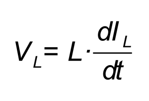
that indicates that the voltage at the inductor’s ends is equal to its value, multiplied for the variation of the current in time.
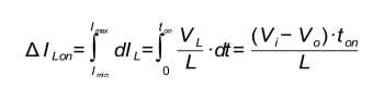
By inverting and integrating the equation, it is possible to obtain the period in which the switch is closed:
And as for the period in which the switch is open:

From these two equations it is possible to notice that, during the switch’s closing time, the inductor’s current grows proportionally to the difference between the input voltage and the output voltage (Vi-Vo) and to the switch’s closing time and inversely with respect to the inductance value.
With a simplification, the greater the difference between Vi and Vo and the closing time, the smaller is the inductance, the more the current grows in output.
During the switch’s opening time, on the other hand, the inductor is unloaded (with a minus sign before Vo in the equation) in a proportional way with respect to the output voltage, and inversely with respect to the inductance value. An aspect that quickly stands out is that the greater the inductance and the less the current growing in the coil, which is translated in less “efforts” in the circuits that surround it, but to a big inductor correspond greater dimensions and/or greater losses due to the electrical resistance of the wire with which it is built (we will talk about this later).
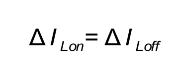
Having considered the hypothesis of a stationary regime, that is to say with constant output voltage and current in the inductor that is never null, we will see that the current accumulated during the switch’s closing will have to be released exactly and entirely during the switch’s opening; therefore we may write that:
That is to say, by substituting with what has been obtained before:

Since we are interested in calculating the output voltage value on the basis of the switch’s closing and opening times, we will solve for Vo :
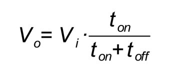
And, by naming D the switch’s duty-cycle (that is to say, the ratio between the time in which it remains closed and the total time):
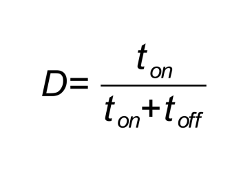
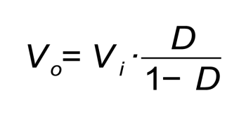
We may write down the final equation of our converter:

Please notice that the D duty-cycle may have values ranging between 0 and 1, therefore the output voltage may be lower or equal to the input one, but never greater, with this type of converter.
For those who know a bit about Arduino world and its PWM outputs, it is easy to think to use a MOSFET in the place of the switch, and to apply a square wave supplied by one of Arduino’s outputs to the gate. For example, by choosing a 25% value for D, we will obtain a quarter of the input voltage as an output.
Someone will have noticed that in our very beautiful and simple equation the inductance, L, has disappeared and therefore it doesn’t influence the output voltage value in any way.
We may therefore choose any value for L? In theory, yes, if we weren’t interested in other factors and, above all, if the inductor was an ideal one, that is to say, without any electrical resistance in the wire composing it.
We already saw before, in fact, that the current in the inductor (and therefore in a great part of the circuit) grows faster with the decrease of the inductance itself and with the increase of the closing time.
Therefore, with low inductance values and/or with long switch’s closing times, the current will grow a lot, with the risk to damage the same components; moreover, great variations in the current correspond to great electromagnetic disturbances, that are generated by the circuit and that end in the powered device.
In contrast, if we increase the inductance too much, it will have a quite high resistance due to the wire (the higher the value, the more wire coils are needed), which will determine losses of the energy that is transformed in heat, and a consequent loss of efficiency of the converter, in addition to a greater size.
Moreover, it is possible to notice that, with all other things being equal (inductance and Vi and Vo values), by decreasing the closing and opening times, the current is kept lower. A decrease in the opening and closing times (when keeping D constant) however corresponds to an increase in the switching frequency; it would be best, therefore, to choose a small inductance and a frequency being the highest as possible.
Unfortunately, even if we are trying to do everything possible by taking advantage of the modern electronic components, there are some impassable limits, both for the frequency with which the same may operate, and for the switching losses, due to the fact that an instant action is impossible.
Even here a compromise between the high frequency and the possibilities given by the components available is necessary; if for a converter having discrete components it was already something extraordinary to reach and exceed a frequency of a few hundreds of kHz, with the modern integrated circuits it is possible to reach frequencies that are greater than a MHz and, in the last years, even greater than 3 MHz.
This is translated in a greater compactness of the power supplies, a greater efficiency and a lesser cost, at the price of a greater attention needed when disposing the components on the PCB, as we will see in the second installment, in which we will present a practical converter circuit.
Efficiency of the switching converter
When analyzing the ideal circuit we talked about until now, the first thing that stands out is that there are no resistive components in it: the energy supplied from the power source goes to load an ideal inductor (thus having a zero ohm resistance) which is then discharged on the load by means of the same and the diode, that is also imagined as an ideal one.
Therefore, all the energy drawn from the generator is transmitted to the load with a 100% efficiency.
A nice step change in comparison to the 60-40-20% of the linear regulator!
Unfortunately, ideal components do not exist: the inductor is composed of a copper wire with a certain resistance, the diode – even if accurately selected – has a certain voltage drop at its ends, the same PCB tracks are in copper and therefore affected by the electric resistance and the switch, that in the 99% of the cases is made of a MOSFET, and has an insertion resistance, albeit a minimal one. In fact, even if the technology of these components made enormous progress in the last decades, the MOSFET has an ohm resistance between drain and source and a switching time that are not null. This is translated in a loss of efficiency, whose calculation falls outside the purpose of this article, and it is verifiable by measuring the absorbed current and the one supplied at the load. The absorbed power is in fact equal to:

while the power returned to the load is equal to:

And the efficiency is given by:

In the actual conditions of our converter, it is always true that Po < Pi and therefore there is an efficiency that is lower than the theoretical 100%. We will see the values in the field when talking about our actual circuit.
The ripple
Until now, we have seen how our converter takes advantage of the inductor for the purpose of storing energy that is then returned to the load at a different voltage, and this is done by means of a switching mechanism, and differently from the linear regulators we saw before.
It is therefore obvious that, among all the qualities of our converter, a great flaw appears: we may see a variable (more or less small) voltage, named ripple, overlapping the direct output voltage.
How small it is? It depends mainly from the value of the output capacity and from the switching frequency; the higher are the values of the said parameters and the lower the ripple will be, with the problems we saw until now, that is to say: encumbering capacity and other problems if we increase the capacitor, and switching problems/technological limitations if we increase the frequency.
Even the inductance and other parameters influence the ripple. We need therefore the usual compromise between values, and for such a reason it is necessary to calculate the ripple and to decide if it is an acceptable value or not.
Unfortunately, an accurate calculation of the ripple is quite a complicated one, and we will see that quite in detail in the final diagram; at the moment, it is sufficient to know that by increasing the capacity and/or the frequency, the ripple decreases.
Increasing the input voltage
The switching converter seen until now is capable of decreasing the generator’s voltage, so to bring it to the one that is necessary for the load, that is to say it is capable of obtaining an output voltage that is lower than the input one; it is therefore named “step-down” converter.
What happens, however, if the need is the opposite one, that is to say if we have – for example – a LiPo battery capable of supplying a voltage ranging between about 3 and 4 volts, and we are in need of the fateful 5 volts?
In this case another type of switching converter may help us, it is named boost converter, that is to say it is a “step-up” converter.
As it can be seen from figure , that schematises it, the difference with respect to the previous principle diagram is that the inductor is found before the switch and that the latter short-circuits it towards ground.

The two operating stages are:
- closed switch; the current flows from the generator (the voltage applied to the converter’s input) in the inductor, thus loading it;
- open switch; the inductor tries to keep the current flow of when the switch was closed, by reacting to the opening with an inverted extravoltage that finds an outlet in the capacitor and that flows in the same direction, and loading the capacity with a positive polarity on the diode’s cathode.

In summary, when the switch is closed all the current supplied from the generator goes to load the inductor, while the load is powered only by the output capacitor; while with the switch open, the inductor is in series with the generator and therefore the voltage to its ends is added to the one from the generator itself, thus increasing it. The diode is needed – in the stages in which the switch is closed and the inductor is being charged – in order to avoid that the capacitor is emptied by the switch itself.
Without having to repeat the previous calculations, and always under the same hypotheses, the equation used for the calculation of the output voltage becomes:
Since D is always less than 1 (the duty-cycle… Do you remember it?) the output voltage will always be greater than the input one.
Output voltage ranging between the minimum and the maximum input voltage
Up to now, we have seen two types of converters, one capable of decreasing the input voltage (buck converter) and the other one capable of increasing it (boost converter). What happens, however, if we need an intermediate output voltage? For example, if we want to power our 5 volt device and sometimes we have a 4.2 V LiPo battery available, and some other ones an external 12 V power supply; or if we have a circuit working at 3.3 volts and we have to power it with a LiPo that supplies 4.2 volts when it is completely charged and 3 volts when it is almost depleted?
An immediate solution is the one to use two converters, and to select by means of a (manual or electronic) commutator the one to be used from time to time; this solution – however – is quite an intricate and problematic one.
Another alternative is the one to use a boost converter, so to bring the input voltage to the maximum accepted value, and then a buck converter in cascade, so to bring it back to 5 volts. In our case, it would be:
![]()
Even this solution is an intricate one, it uses two complete converters and doubles the power losses, thus reducing the total efficiency.
There are buck-boost converters that allow to obtain whichever output voltage but, if they are not isolated from a transformer, the voltages are obtained with an inverse polarity with respect to the input one, which is often unacceptable.
Among the various implemented types, one recently emerged: it is named SEPIC, and was mainly encouraged by the arrival of the LiPo batteries that, as we just said, supply a voltage that is 4.2 V when fully charged and at the end-of-charge they even go under 3 volts; it was born in order to power devices that require 3.3 volts, that is to say a voltage that is between these values. Even here, this is the case of an intermediate output voltage among the possible input values, even if the window is smaller.
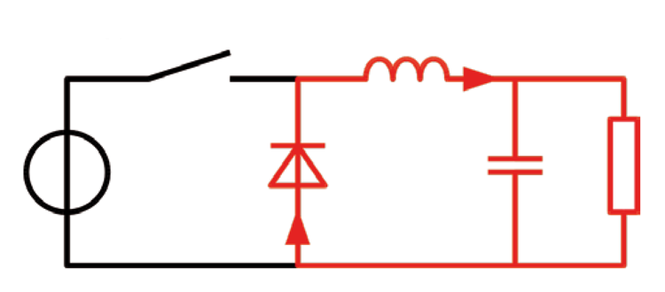
The SEPIC converter
The principle diagram of the DC/DC SEPIC converter is shown in figure : in comparison to the previously seen converters, it is possible to immediately notice the double inductor and the C1 capacitor, that represent the “complication” with respect to the other ones.

A positive note concerning the buck converter is that in this one, if the switch short-circuits, all the input voltage ends on the load, that has many odds of taking damage; on the other hand in the SEPIC – thanks to the C1 capacitor – the generator’s DC component is blocked and, in the case of malfunction, the output voltage is zeroed, thus protecting the powered devices.
However, the functioning is decisively much more complex and deserves a detailed analysis; let’s start by examining the functioning in continuous mode (CCM) that is obtained when the current in the L1 inductor is never zeroed; even here, the discussion converning the functioning in the discontinuous mode will be omitted.
In conditions of stability, the average voltage at the C1 (VC1) capacitor’s ends is equal to the input voltage (VIN). Since the C1 capacitor blocks the continuous component, the average current flowing through it (IC1) is null, thus the L2 inductor turns out to be the only source of direct current for the load.
Therefore, the average current that flows through the L2 (IL2) inductor is the same of the average current on the load and therefore it is independent from the input voltage.
By analyzing the average voltages on the circuit, we may write as follows:
VIN = VC1 + VL1 + VL2
and, since the average voltage, VC1 is equal to VIN:
VL1 = –VL2
This makes it possible to wind up the inductors on a single nucleus, given that the previous equation says that the influence of the mutual inductance between the two is null.
It won’t be our case – for problems of availability of the components – but this represents a great advantage at an industrial level.
Even the peak currents in the two inductors will be equal as an absolute value.
The average currents may therefore be expressed by:
ID1 = IL1 – IL2
with the average current in C1 being null.
When the switch is closed we have the condition depicted in previous figure
The input voltage charges the L1 inductor, while the L2 inductor is charged by C1’s voltage that, as we said, is equal to the input voltage, in the beginning.
Please notice that, arithmetically speaking, the two currents flowing into L1 and L2 are opposite, i.e. the current that charges the L2 coil has a “negative sign”: so, actually, the charging current is “discharging” the coil during this phase.
By opening the switch we reach the situation depicted in figure: since the L1 inductor makes it impossible to have an instant variation of the current, all the current flowing through L1 will have to forcedly flow through C1 as well. The current in L2 will continue flowing as before in the opposite direction, but this time it will flow through the load (red line in the diagram shown in figure). We will see therefore a negative current (IL1) that will be added to the IL2 current.
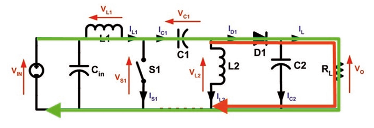
From Kirchhoff’s Law, applied to the nodes, we obtain the following relationship:
ID1 = IC1 – IL2
therefore the current at the load, with the switch open, is supplied by both L2 and L1, while the C1 capacitor is recharged by L1.
In summary:
- with the switch closed, the power source charges L1, while C1 charges L2;
- with the switch open, the L1 and L2 inductors power the load, while L1 recharges C1.
During the operations, the voltage on C1 may change its sign , therefore we need to insert another component: a non polarized capacitor.
The converter’s functioning may be seen as the coupling of a boost converter, composed of L1 and the switch, that generate a VS1 voltage that is greater than the one of the power source; it is followed by a buck converter that reduces VS1 to the required value.
Since the voltage at C1’s ends is equal to VIN, as previously seen, the output voltage becomes:
VO = VS1 – VIN
Therefore if VS1 is less than twice the amount of VIN the output voltage will be lower than the input one, in the opposite case it will be greater.
Without going further into detail, the equation regulating the relationship between input and output voltage is equal to:
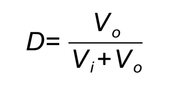
in which D represents the usual duty-cycle, that is to say the ratio between the times of the switch being closed and the total time (open + closed switch).
From here it is possible to extract:
That shows how the output voltage is lower than the input one with D < 0.5 and it is greater with D > 0.5.
The abovesaid formulae are true, as usual, in the absence of dissipating (resistive) components and/or non linear ones (MOSFETs, diodes, etc.) in the circuit, which is something that is not true, in practice; for example, we have to consider the voltage drop on the diode, the coils resistances, the capacitor’s ESR, etc., that contribute both to slightly modify the formula and to decrease the efficiency.
From openstore

Related Posts


-
 Arduino ISP (In System Programming) and stand-alone circuits
We use an Arduino to program other ATmega without...
- Posted 12 years ago
-
-
-
 GSM GPS shield for Arduino
Shield for Arduino designed and based on the module...
- Posted 12 years ago
-
 Small Breakout for SIM900 GSM Module
Some post ago we presented a PCB to mount...
- Posted 13 years ago
-
 Join Maker Faire Rome 2024: Innovation Unleashed at Gazometro Ostiense | Calls Now Open!
All Calls Now Open for Maker Faire Rome 2024...
- Posted 3 weeks ago
-
 Building a 3D Digital Clock with Arduino
Project to create a digital clock consisting...
- Posted 4 months ago
-
 Acoustic amplifier – in DIY Kit
This kit creates a microphone amplifier with an output...
- Posted 5 months ago
-
 Creating a controller for Minecraft with realistic body movements using Arduino
Project of a controller that maps body movements...
- Posted 5 months ago
-