Bench instrument capable of generating sine, square, rectangular, triangular and sawtooth waves. It works at a frequency between 50 Hz and over 5 kHz and is based on the ICL8038, a chip capable of performing all tasks requiring very few external components.
On the electronic workbench, in addition to the tester and a soldering station, there should be measuring instruments such as the oscilloscope and the signal generator (or function generator, if you like); the latter can be built without particular effort or large costs and to prove it, we publish in these pages the project of a generator of “essential” waveforms useful for carrying out the various analyzes and measurements on linear circuits, such as power amplifiers and voltage (preamplifiers) but also on audio devices and filters.
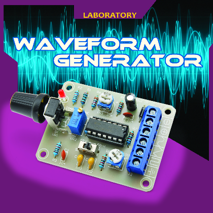
This is an easy-to-create project created taking into account the needs of experimenters, who often have little money to spend and who do not lend themselves to SMD assemblies that today are also rampant in the pages of electronics magazines. In short, a generator for everyone, based on one of the most tested integrated circuits, namely the Harris ICL8038, which vaguely recalls the older and more famous MAX038 from Maxim. The integrated ICL8038 is capable of generating sinusoidal, triangular and square wave output signals in a wide range of frequencies ranging from 0.001Hz to 300 kHz, but in our generator, we simply work from 50 Hz to 5 kHz.
But let’s analyze the circuit of the waveform generator, which is then summarized in the integrated ICL8038 and in the very few contour components, since the chip carries out practically everything inside, requiring only the potentiometers and trimmers to set fields of frequency and other adjustments.
Electrical diagram
The heart of the circuit is the integrated U1 which, powered by the direct voltage coming from J1, turns on and starts generating its own basic waveform thanks to the internal oscillator if we can call it that, which is a generator of triangular and rectangular unidirectional wave based on flip-flops.
Everything originates in a block that operates the constant current charging and discharging of the timing capacitor connected between the TCAP pin (pin 10) and GND (pin 11), determining a fairly precise triangular component, since the capacitor is charged and discharged through a constant current generator and therefore the charge and discharge curve is straight.
Components List:
R1: 200 ohm 1%
R2, R3, R4: 10 kohm 1%
R5, R6, R7, R8: 33 kohm 1%
VR1: 5 kohm potentiometer
VR2: Multi-turn trimmer 5 kohm
VR3: 20 kohm trimmer
VR4: 100 kohm trimmer
D1: 1N4007
D2: LED 3 mm red
C1, C2: 100 nF ceramic
C3: 10 nF ceramic
C4: 1 nF ceramic
C5: 220 µF 10 VL electrolytic
U1: ICL8038
S1: Slide switch
Misc:
- Socket 7 + 7
-
Potentiometer knob
-
3-way terminal (2 pcs.)
-
Printed circuit board S1464 (59×44 mm)
The block composed of the two internal voltage comparators, which compare the potential on the capacitor with two reference voltages: decides when to stop charging to start the discharge: when the potential reaches the high threshold, the respective comparator switches going to intervene on the internal CMOS switch that switches the capacitor and therefore the TCAP foot, from the output of the constant current generator used in charge to the constant absorption load which, from this moment, operates the discharge.
As soon as the voltage drops below the lower threshold, the other comparator intervenes by piloting the internal switch with its own output so that it switches over again.
The outputs of the comparators, therefore, work by alternating their logic levels and in the integrated circuit they are used to control the inputs of an RS flip-flop, whose output produces a rectangular wave.
The voltage drawn at the ends of the timing capacitor constitutes the triangular wave and is sent to the input of a buffer which makes it available at the dedicated (triangular) output or at pin 3 (TW = Triangular Wave) while the flip output -flop goes to a second buffer, which makes it available at pin 9 (SQW = SQuare Wave). Then the triangular and square waves come out of the integrated directly and are generated directly.
Instead, the sinusoidal is obtained by means of a “sine-shaper” circuit, that is, a sinusoidal modeller that receives the triangular wave at the input and obtains a sinusoid; this circuit consists of a particular common base multistage amplifier with cascade elements, feedback to each other so as to progressively saturate, or to limit the gain as the triangular amplitude grows, so as to shape it, precisely, giving the sinusoidal envelope.
The shaping stage, visible at the bottom right of the integrated circuit diagram shown in Fig. 1, internally takes the triangular signal present on pin 3 (the output of the triangular buffer) and supplies its signal to pin 2 (SWO, that is Sine-Wave output) with respect to mass; it is possible, through the voltage applied to pin 12 by the VR4 potentiometer (inserted in the resistive divider which also includes R7 and R8), to modify the envelope of the sinusoid within certain limits, to give it the best possible shape. The adjustment can be done visually by looking at the signal on an oscilloscope, or more precisely by using a distorsiometer.
The internal circuitry of the ICL8038 adopts solutions to ensure the production of a fairly linear sinusoidal signal and similar (if not equal) to that obtainable by a phase-shift oscillator.

Fig. 1
An interesting feature with which the Harris chip is equipped is the sweep, in the sense that by means of a control voltage supplied from the outside to the FMSWP pin (8) it is possible to frequency shift the signals produced up or down because the relative control acts directly on the charging and discharging times of the timing capacitor.
Note that since the integrated does not cover the entire frequency range of which it is capable with a single capacitor, we have divided the field into two ranges, mounting two capacitors in the circuit connected with one electrode to the ground and the other each at one end of a single-pole diverter (initialled S1 in the wiring diagram) whose common electrode is connected to pin 10, which is that of the timing capacitor.
In terms of timings, we can explain the role of the VR3 trimmer and of the resistors R5 and R6, which form the group of resistors which act on the constant current generator which operates the charge/discharge of the capacitor connected between the TCAP pin and ground: l The integrated allows to separately manage the charging and discharging times and therefore operate a variation of the duty cycle of the rectangular wave, ranging from a minimum of 2% to a maximum of 90%; to be precise, the charging time and therefore the high-level impulse of the rectangular wave (i.e. the ascending ramp of the triangular) depends on the resistor connected between the power supply positive of the integrated circuit (pin 6) and the pin 4, while the one at the low level (descending ramp of the triangular) is correlated to the value of the resistor connected between the power supply positive and pin 5.
Calling Ra the resistor connected to pin 4, the relationship holds:
t1 = (Ra x C) / 0,66
where C is the timing capacitor inserted and t1 the duration of the charge of the same and therefore of the high level at the SQW output.
Instead, the duration of the low-level impulse and therefore of the capacitor discharge is determined by:
t2 = (Ra x Rb x C) / 0.66 (2Ra – Rb)
in which Rb is the resistor connected to pin 5.
With two completely separate resistors, the working frequency is valid:

Or, if the resistances are equal, the frequency is valid:
f = 0,33 / R x C
where the value R is equal to Ra and Rb.
In our circuit we preferred to keep two resistors the same, but connected to the positive supply via a trimmer that has the cursor at the positive and connects to the resistors at the two ends: this solution allows you to assign to each of the R5 (Ra) and R6 (Rb) a variable portion of the resistance of VR3 depending on the position taken by the cursor and, to be exact, equal to the cursor in the centre, greater than R5 by moving the cursor towards R6 and vice versa. Translated into practice, cursor in the centre means a square wave, cursor towards R5 a rectangular wave with gradually decreasing duty-cycle as you approach the R5 itself and cursor towards R6 corresponds to having a rectangular waveform with increasing duty-cycle the closer you get to the R5 itself.
Note that the configuration adopted by us is the simplest which allows us to vary the duty cycle of the signal produced by keeping the frequency constant, that is, without the regulation changing the frequency; in fact, if only one of the resistances is changed at a time, the only time for charging or discharging the timing capacitor changes, so that the square wave is no longer such but becomes a rectangular one, with a duty cycle different from 50%. But above all, the length of the period changes, which implies that the frequency produced varies, which is not permissible during certain measurements.

It goes without saying that by varying the duty cycle of the signal present at the SQW output, the sinusoidal and with it the triangular is deformed; more exactly, reducing the duty cycle tightens the “positive” half-wave of the sinusoid and instead, the square becomes a sawtooth.
In the circuit, the working frequency varies with the VR1 potentiometer, because it supplies the control voltage to the FMSWP sweep input; with the VR2 trimmer, it is possible to adjust the range.
The deviation of the frequency obtainable with the voltage applied to the pin 8 is to be understood with respect to the basic value set with the group R5, R6, VR3 and the timing capacitor chosen by means of the single switch S1: with the trimmers in the centre, it is exactly that while bringing the cursors towards the positive of power increases since the frequency is directly proportional to the potential applied to the pin 8. Therefore, by bringing the cursors towards the ground, a decrease in frequency is obtained with respect to that at rest.
Note that the trimmer allows you to limit the range of action of the potentiometer, calibrating the sweep finely, while the potentiometer performs a coarse adjustment, then to set the frequency, first you go around the desired value with the VR1 potentiometer and then with the trimmer you adjust the value.
Well, that said, we can conclude the analysis of the wiring diagram with the power supply, which is typically 12 volts and is applied to connector J1, precisely on pins 1 (negative) and 2 positive; this voltage exceeds the diode D1, which serves as protection in case of polarity inversion) and suitably filtered by disturbances and any residual AC power supply residue, reaches pin 6 of the ICL8038. The LED D2, whose current is limited by the resistance R2, when it lights up it indicates when the circuit is live and therefore operational (we can mount it on the front panel once the instrument has been made).
Adjustments and use
The waveform generator, once assembled and boxed, is immediately functional, however, it is advisable to go at least to adjust the distortion of the sine wave, since this signal is obtained from a shaping circuit, whose operation is optimized thanks to a careful adjustment of the VR4 trimmer; the latter intervenes, as you can see in the internal diagram of the integrated proposed in Fig. 2, on the basic polarization of the transistors making up the sinusoidal profiler and allows for distortion of even less than 1%, which, considering the type of integrated and its commercial target, is an excellent result.
However, the adjustment must be made by connecting the probe of an oscilloscope between the ground and the sinusoidal output of the circuit and setting the time base and sensitivity (V / div.) So as to display the largest possible wave; at this point, the cursor of the aforementioned trimmer is rotated in one direction and the other until a wave that is as harmonious as possible, i.e. as less distorted as possible, is obtained. Once this is done, the circuit can be considered calibrated.
When using the generator, it should also be considered that the triangular and sine wave outputs have a rest voltage, i.e. an offset which must be taken into account if you are driving DC-coupled circuits; in fact, the waves you see in Fig. 2 were obtained by setting the AC coupling in the oscilloscope and therefore refer to the zero volt axis, but in reality, they oscillate around the continuous value present in rest conditions.
In order to obtain a signal without polarization voltage from the generator, the triangular and sinusoidal outputs must be coupled by means of an electrolytic capacitor, possibly of good quality and therefore tantalum, of 47 µF, a value that should ensure a good response with loads at the impedance output included in the range admitted by the integrated, considering that the internal output impedance is 200 ohms.

Fig. 2
No coupling is required, however, for the rectangular wave, since it oscillates between zero volts and the peak value, which is slightly lower than that of the integrated power supply potential; however, a capacitor would significantly alter the waveform, tilting the pulse levels to decrease over time.
Conclusions
The generator proposed here is a project designed for those who have to perform tests on low-frequency circuits without too many pretensions: it is assembled quickly and easily and can be used just as easily, without any problems. It is also a good base, which can be processed for more powerful performance.
From openstore
