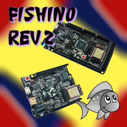
Our Fishino boards are evolving, acquiring new and exciting features and functionalities. The renewal starts with UNO and MEGA. We are now going to explain to you what has changed.
In the previous article, we introduced what would become the founder of a series of innovative boards compatible with the famous Arduino: the Fishino UNO. This board was soon followed by Fishino Mega and, later, by Guppy and two 32-bit boards, Fishino32 and Piranha. When we designed the Fishino UNO and the Mega we wanted to maintain full compatibility with the corresponding Arduino models, using the same controllers and, for additional peripherals, the same I/Os used by similar Shields available on the market.
Over time, the microcontrollers evolve, and our boards cannot remain insensitive to evolution, so we started to modernize them, giving rise to versions 2 (or REV 2, if you prefer) of Fishino UNO and Mega, with exciting changes that further improve the use and solve some problems, mainly related to some I/Os used by internal devices.
Let’s start with introducing you our wholly redesigned Fishino UNO board.

Fishino UNO REV2
Our progenitor board was the only one without a switching power supply and without the possibility of being powered by a rechargeable battery. The first thing we did was to equip it with the same power supply as the Mega, or a double switching consisting of a SEPIC converter to obtain the 5V from an input that can range from 3.5 to 25 volts, with an efficiency of almost 90%, without the problems of overheating and current limits of a linear regulator, followed by an additional synchronous buck converter for the 3.3 volts, needed for the Wi-Fi module and the MicroSD card.
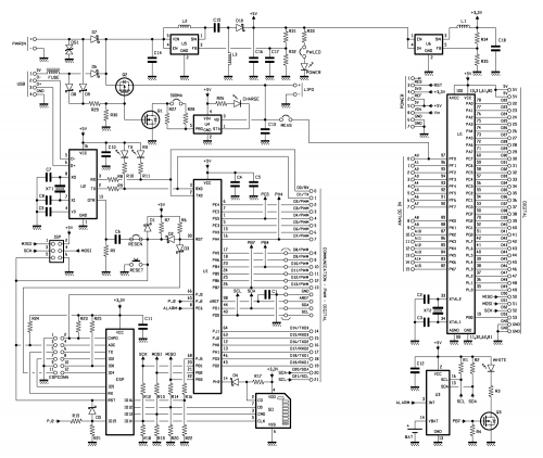
The wiring diagram visible in these pages shows this section, consisting of U4 for battery charging and power inputs, which carry three voltages:
-LIPO, which serves the connector for the rechargeable lithium polymer battery;
-USB, which serves the micro USB connector;
-PWRIN, which serves the power plug.
The two usually higher voltages that of USB and PWRIN are passed through the two Schottky power diodes D6 and D7, while the “lower” voltage, for efficiency reasons, is routed to the MOSFET channel P signed Q3. New to the REV2 is the presence of the DS1 surge suppressor on the PWRIN line.
D6 and D7, together with the protection diode of Q3, form an OR power port, which allows obtaining the highest output voltage among those present at the inputs. For example, suppose to have only the voltage LIPO, about 3.7V: in this case, the diode inside the MOSFET is polarized directly, leading to the converter the same voltage, which cannot return to the other two inputs because of the presence of diodes D6 and D7 polarized inversely.
Now, if we connect the micro USB connector, the 5-volt VUSB voltage directly polarizes the D6 diode and reaches the converter while the diode inside the MOSFET is with a voltage of 4 volts at the anode and 5 volts at the cathode and is therefore polarized inversely, blocking the electric current flow.
If, finally, we supply also the PWRIN input with a voltage higher than 5 volts, for example, 15 volts, the diode D7 will be directly polarized, bringing the voltage VIN to the converter, while the diodes D6 and the one inside the MOSFET will be polarized inversely, blocking the electric current flow.
The stage in question thus achieves the objective of fully automatic switching of the power source.
Let’s now return to the MOSFET Q3, necessary to bypass the small voltage drop of the Schottky and reduce power losses, which become significant at high currents.
The voltage selected by the diode OR reaches pins 4 and 5 of the U5, which is the basis of the SEPIC converter, whose main advantage is the possibility of obtaining both lower and higher output voltage than the input one, thus combining the advantages of a Buck converter and a Boost, just by using a single integrated unit switching.
The output voltage is regulated by the R29 and R30 divider, which provide a reference voltage of 0.6 volts at the FB input of the integrated unit when 5 volts are present at the output.
At the output of the SEPIC converter, there is, therefore, a DC voltage of 5 volts. The green POWER LED acts as a power indicator and can be deactivated by cutting the SMD LEDON jumper, to reduce consumption to the limit if you want to supply the Fishino UNO with battery power. The 5-volt output voltage of the SEPIC enters another switching converter, this time a simple Buck (or step-down) converter operating at a frequency higher than MHz which, for efficiency reasons, has been realized through a synchronous converter, that is equipped with a second MOSFET inside instead of the Schottky diode customarily used. From this converter come out the 3.3 volts, necessary to power the Wi-Fi module and the microSD reader. The battery is recharged by U4, the usual MCP73831 in the classic configuration necessary to keep a lithium polymer cell charged. The PROG pin is used to set the charging current, which depends on the resistance connected between PRG and ground; in our circuit it can be chosen between two values: about 100 mA with the jumper marked 500 MA open (only the 10 kiloohms R9 resistance is inserted) or about 500 mA with the jumper closed.

The LED CHARGE indicates the charging state of the battery, although it should be noted that due to the inaccuracy of the internal detector, especially at low supply voltages, it can turn on the LED even when the battery is charged (while it must remain lit only during charging); do not worry, this is a normal behaviour.
Note that we are using the MOSFET Q2 to close or leave the U4’s PRG pin open so that the charger is turned off when the circuit is not powered by either the USB or the PWRIN jack. The usual MEAS jumper allows connecting the microcontroller analogue input ADC0 to the battery if we need to check the charging state.
Let’s leave the power supply stage and move on to the microcontroller, which here, in the Fishino UNO REV2, is no longer the ATmega328p, which has been replaced by its evolution ATmega328pb. The latter, while remaining 100% compatible with its predecessor, has some additional peripherals and I/Os that we readily used to manage the Wi-Fi module, the microSD card and more, without committing the I/Os available on the external headers. Thanks to this choice, we were able to free up the I/O 4, 7 and 10, previously intended for these devices, thus avoiding any interference with external shields; we also used a couple of internal I/Os for new functions, which can be used alternatively with each other:
- alarm management by RTC;
- Wi-Fi module switching off and microcontroller waking up;
- additional I²C port.
Before seeing how to take advantage of these features, let’s make a premise: to use the REV2 of our boards it is essential to install the Fishino package in the Arduino IDE; not doing so, the board can still be used as an Arduino UNO, but it will not be possible to take advantage of the built-in peripherals such as the Wi-Fi module and the MicroSD card, which the UNO does not have and which usually occupy the additional ports of the microcontroller.
Internal peripheral management (Wi-Fi and microSD)
As mentioned above, some internal I/Os are now used to manage these peripherals, thus freeing up the previously used pins 4, 7 and 10, which are then made available for any other use. Instead, the 3 I/O for the SPI interface is still used and can be used simultaneously by other SPI devices as well.
The only “drawback,” if you want to call it that way, when using the additional internal I/Os, is that the Wi-Fi selection pins (WIFICS, first pin 10) and microSD (SDCS, first pin 4) change their nomenclature and become, respectively, I/O 23 and 22.
In sketches, therefore, it is no longer necessary to use the numbers 10 and 4 but the WIFICS and SDCS constants, already correctly defined in the various libraries.
For example, the instruction for initializing the SD card changes from the following:
card.init(SPI_FULL_SPEED, 4);
to this one:
card.init(SPI_FULL_SPEED, SDCS);
The WiFi module is managed, instead, directly from the Fishino library, so you don’t need to modify anything in that case.
SPI, I²C and USB interfaces
The SPI section is the same as the Fishino UNO. Its function is to adapt the ATmega’s 5-volt logic levels to the 3.3-volt levels of the Wi-Fi module and microSD card. The adaptation is made simply through resistive dividers (resistors from R7 to R17) in the direction 5V -> 3.3V, while in the reverse direction the 5 volts logic considers as high values signals that are much lower than 3 volts, thus being compatible with the 3.3 volts logic. The MISO (Master In Slave Out) signal apparently does not require an adaptation, since the direction goes from the 3.3 volt logic to the 5 volts one, but we have to consider that using the remote programming via Wi-Fi (OTA), the master and slave roles are reversed, and the MISO becomes an output (5V logic of the Atmega) to the Wi-Fi module (3.3V logic).
The MicroSD interface works through SPI lines including MOSI (data from ATmega to SD, Master Out Slave In), MISO (data from SD to ATmega, Master In Slave Out) and SCK (clock). The levels to the SD card are reduced by the level adapters mentioned in the previous paragraph.
The card selection is made through the PE2 line of the microcontroller, which is adapted to the voltage level required by contact 2 of the SD card reader through R1 and D1 (one Schottky); the SD is activated with the PE2 at low level, while with 1 logic or three-state (high impedance) it is disabled.
New to the REV2 is the addition of a second I²C-Bus interface which is available using the Wire0 peripheral (as opposed to Wire which is the main I²C interface); its I/Os are available on the ESPCONN connector, added to the REV2, as shown in Fig. 1.
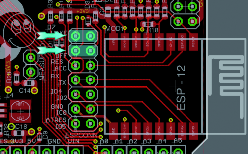
Fig. 1
This interface uses I/O 20 and 21, superimposed on other functions (alarm input and low power management), so it must be used as an ALTERNATIVE to these; i.e. if you want to use Wire0, you cannot use the RTC alarm and the management of shutdown of the Wi-Fi module.
The Wire library contained in the Fishino package is already ready to manage the additional I²C.
Please note that the Fishino UNO REV2 does not have the two pull-up resistors necessary for the I²C interface; if your peripherals do not have them (usually there are…) you must connect two resistors of 4.7 ÷ 10 kiloohms between these pins and the positive (+5V) power supply.
Let’s move on to the USB interface, which is the same as the original Fishino UNO and develops around the integrated CH340G; the chip was chosen both for economic reasons and circuit simplicity, considering the same performance.
The integrated unit provides all the signals of a standard RS232 interface at the output, of which we only use the data transmission/reception signals (RX and TX) and the DTR signal used for automatic reset during programming, exactly as in the original Arduino, which allows loading the sketches without having to press buttons or operate any switch.
RTC section
The RTC module has evolved as well; the relative chip, a DS1307, has been replaced with a DS3231, considerably more precise, equipped with an alarm output and with built-in quartz, which allows its precise calibration during production and any software corrections that may be necessary to compensate for ageing.
The RTC alarm output can be connected to input 20 (one of the additional I/Os) using a jumper on the PCB (Fig. 2) which allows the activation of the RTC alarm (a new functionality of the REV2).
Inserting this jumper at digital input 20 (readable with a digitalRead(20) instruction or usable as a “pin-change” interrupt input) will generate an impulse each time the RTC alarm is activated.
The FishinoRTC library is already predisposed to manage this input and to correlate it with a function called up at the end of the alarm; to obtain further details you can read the FishinoRTC.h file of the library itself, waiting for it to be documented.
The alarm input is shared with the Low Power functionalities, as explained in the following paragraphs, and is also used by the FishinoLowPower library to allow the Wi-Fi module to wake up the board after a sleep period; therefore, using it to manage the RTC alarm you will have to renounce to wake up from the low-power. The input is also shared with the additional I²C interface, as we will see below.

Fig. 2
Wi-Fi section
The Wi-Fi module is the same as the original Fishino UNO; communication with U7 takes place via the SPI interface and using some circuit devices such as the D2 diode, used to force the module’s IO15 pin to reset at a low level, without it the module itself would start in the “loading from SD” mode, which would make it pretty much unusable. This is necessary because GPIO15 also has the function of Slave Select (SS) of the module and therefore cannot be directly grounded.
All the useful pins of the module are carried on a connector (ESPCONN) as shown below.
- GPIO0: in addition to being used as a digital input/output, it is used to select the boot mode at module boot. The latter can be started from the internal Flash (normal operation, GPIO0 to 1) or the serial interface, used for firmware reprogramming (GPIO0 to 0).
- GPIO2, GPIO4, and GPIO5 are available for being used as digital pins and can be accessed through the appropriate library functions as if they were digital pin extensions of Arduino.
Rx and Tx create the module’s hardware serial port and are also used during firmware programming. A future firmware extension will make them usable as an additional serial port that will allow Fishino UNO to have an additional serial port.
- CH_PD is the module enable pin. If you set it to a high level, the module is enabled (default setting), while a low level puts the ESP in standby mode, reducing its power consumption to almost zero.
- RESET is the hardware reset of ESP, active at a low level.
- ADC is the analogue input of ESP, directed to a 10-bit A/D converter (1,024 possible values).
The Fishino UNO REV2 reset section remains that same as the original Fishino UNO one that you already know and provides for the simultaneous reset of the U7 and the Wi-Fi U1 module at the reset button press, at the start and the programming request by the IDE; to be able to perform the programming of the Atmega via Wi-Fi, the ESP module must be able to reset the Atmega itself without being self-resetted.
Let’s start with the DTR signal that exits the USB/Serial interface (U1/CH340G) and that, as mentioned before, is set to a low level when the serial port is opened. Through the C5 capacitor (1 µF ceramic, against the 100 nF of the original to lengthen the reset pulse) a short pulse is generated which, passed through the SMD RESEN jumper (cutting which can deactivate the auto-reset), reaches the “external reset” line, to which are also connected the reset button and pin 5 on the programming connector (ICSP). Unlike the original circuit, in the Fishino boards, between the RESET line and the corresponding pin of the Atmega, there is the diode D10, whose purpose (and that of the diode D10) is to reset only the Atmega, without transmitting the signal also to the ESP.
Through this system, we have therefore given the possibility to the Wi-Fi module to control the reset line of the Atmega that, together with the SPI interface, allows its reprogramming without even the need for a preloaded bootloader. In practice, with minor changes to the firmware, it would be possible not only to reprogram via WiFi the Atmega but also to use the space generally reserved for the bootloader; we have not implemented this yet because, in case of any programming errors, we would risk to find ourselves with a no-bootloader board. We will implement it later, however, with all the necessary care!
As for the previous version, you can load the sketches via Wi-Fi (firmware update OTA), but in REV2 we have relocated the connectors so you can enable it through a simple jumper, as you see in Fig. 3.

Fig. 3
Once you have installed this jumper and activated OTA mode during the firmware update, you can comfortably load your sketches via Wi-Fi using the Arduino IDE or our FishIDE development environment.
Low consumption characteristics management
In the FishinoUNO REV2, we have set up some I/Os that can be used by the FishinoLowPower library so as not to occupy external resources; in particular, the reset functions of the Wi-Fi module and automatic awakening of the board through its internal RTC can be managed through internal I/Os.
To activate these functions, two jumpers must be inserted as shown in Fig. 4.
Fig. 4
Once these jumpers are inserted, the FishinoLowPower library will be fully functional, while neither the additional I²C interface nor the RTC alarm management can be used.
The upgrade procedure is simplified by a program available for both Windows and Linux platforms, which operates fully automatically and is error-free. The steps for updating are as follows.
1) Load a sketch that does not use the serial port; the basic example BLINK (the one that causes the LED on the board to flash) is perfect. This step is used to avoid interference between the loaded sketch and the serial connection via Atmega and ESP. If the flashing program does not detect Fishino, a wrong sketch has been loaded almost certainly.
2) On the ESPCONN connector you have to connect the Fishino TX line with the ESP-TX line and the Fishino RX line with the ESP-RX line (refer to Fig. 1):
- connect the GPIO0 port to the ground using a cable or a jumper, always on the ESPCONN connector (Fig. 1);
- connect the Fishino to the PC (or press the RESET button if already connected);
- launch the FishinoFlasher program, making sure your PC is connected to the Internet.
If the connections have been made correctly, the program will detect the port to which Fishino is connected, determine the model and version of the firmware currently installed, connect to a remote server and download the list of available firmware, showing the latest and still allowing the selection of previous versions, in case you want to downgrade (Fig. 2). Clicking on the “Flash” button will start the update process, at the end of which a confirmation message will appear. To end the program, press the “Exit” button. If Fishino is not automatically detected, you can try to select the port manually. However, it is likely that some errors have been made in the connections. Manual selection is essential only when more than one Fishino are connected to the PC at the same time, in which case the first one is automatically detected, but it is still possible to choose another one. Once the procedure is complete, remove the three connections and Fishino will be ready to be used.
Battery voltage measurement
To measure the Li-Po voltage through the ATmega internal ADC, we have provided a jumper that connects the battery directly to the analogue input AD0; by inserting this jumper, shown in Fig. 5, the voltage will be measured directly through an analogRead(A0). The microcontroller used, the Atmega 328pb-an, has remarkable additional features, including additional timers, additional PWM, etc. Unfortunately, space here would not be enough to list them all, so we invite you to read the micro datasheet. The additional PWMs on the board headers have been marked, as usual, by the character ‘#’ (deleted).
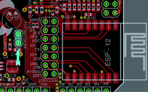
Fig. 5
Fishino Mega REV2
Now let’s move on to the new Fishino MEGA and its wiring diagram, from which you can see how the changes are less consistent and limited to the exploitation of some I/O of the microcontroller, unused on the first MEGA, to manage the internal devices and some additional features. Also, in this case, you should remember that to use the internal peripherals (Wi-Fi and SD Card) and some other features, it is essential to install the Fishino package in the Arduino IDE and select the Fishino MEGA REV2 board; using the board as an Arduino MEGA, the extended features will not be accessible.
The microcontroller remains the same as the original Fishino MEGA (ATmega 2560-16AU) and so remains the USB interface, which you see based on the usual CH340G, already described for the Fishino UNO REV2. The reset section and the circuitry related to the bootloader loading start are unchanged, similar to the Fishino UNO REV2 section, where the manual reset button and the jumper (RESEN) that enables the USB/serial converter reset from DTR stand out.
RTC module
Let’s start with the most apparent modification that is the replacement of the RTC with the DS3231: this device integrates very precise and calibratable quartz and alarm output. Unlike Fishino UNO, here you do not need to use any jumper to enable the alarm functionality, as the available I/Os not used previously are already sufficient to manage all the additional features.
The FishinoRTC library is already able to manage all the functions of the new RTC, including the alarm.
Internal I/O for Wi-Fi and microSD
As for the Fishino UNO REV2, I/O 4, 7 and 10, previously used for the microSD card and the Wi-Fi module, have been released; the pins of the SPI interface (50, 51 and 52) are still used simultaneously on other SPI devices.
To manage SD and Wi-Fi you just need to replace in the sketches, if not done previously (in all our examples you will always find the constants and not the numbers directly), the I/O 4 and 10 respectively with SDCS and WIFICS, everything else remains unchanged.
Internal I/O for Low Power functions
The FishinoLowPower library features require the use of 2 I/Os to manage the shutdown of the Wi-Fi module and the awakening of the Atmega via the RTC inside the Wi-Fi module itself; in the previous version of the board were needed 2 external jumpers and the consequent commitment of 3 I/Os on the board, which are now no longer needed.
The FishinoLowPower library can control, immediately and without any jumper on the board, the energy-saving features available.
Loading sketches via WiFi (OTA)
As for the previous version, it is possible to load the sketches through Wi-Fi; in the REV2 we have repositioned the connectors so that we can enable it through a simple jumper, as you can see in Fig. 6.

Fig. 6
Overvoltage protection
Using very long power cables on the VIN input (header) or the power plug, it is possible that when the power supply is switched on and/or off, high voltage spikes (pulses) are generated due to the excessive inductance of the cables themselves, capable of burning the input converter. This is a somewhat rare occurrence, but it has happened on a couple of occasions (on a few thousand boards in circulation), so we have provided a suppressor diode of extra voltages on the ‘external power supply, able to short-circuit to ground any extra voltage. In the MEGA REV2, we have inserted the DS1 suppressor to protect the line of the PWRIN power jack.
Conclusion
We have finished the presentation of our 8-bit Fishino boards updated versions; all the available libraries and packages of the IDE have already been updated, where necessary, to manage them optimally. We are not going to describe the practical implementation because, even if we report the assembly plans and the list of components in this article, the boards construction is very complex, using double-sided PCBs with densely populated metalized holes, moreover with tiny SMD components, whose positioning requires special equipment that not everyone has. If you want it, you can also realize your REV2 by yourself; for all the others, as usual, the boards are available already assembled and tested at Open Electronics, which provides them with bootloaders in the microcontroller and then ready to receive your sketches, of course from an IDE with the Fishino package loaded.
From open store
