
Thanks to an innovative module, it analyses the electrical grid parameters and the consumption, by supplying them – via USB – to a computer, on which a dedicated software enables to display, collect and use the data for different applications. First installment.
It is common to worry about how much electrical energy is consumed, at home or at work. In order to carry out the measurings as for voltage and current, in addition to the related measures concerning the power absorption and the power consumption, we take advantage of a series of tools that have been designed for this purpose. It may be some simple lab tools, such as for example a voltmeter or an amperometer, so that the different electric power quantities may be manually calculated, or maybe some more sophisticated tools such as the Power Meters (for example, the WT230 by Yokogawa, or similar ones) that autonomously calculate the apparent/real/reactive power, the cosφ (power factor), the network frequency, etc.
Moreover, different measuring instruments for the DIN rail are available for sale (that’s the ones you may mount in your electric panel), they carry out the measurings for the electrical quantities and calculate the apparent/real/reactive power and the amount of energy absorbed by the network.
The purpose of this article is the one to show you an integrated circuit manufactured by Microchip. More precisely, that’s the MCP39F511. Thanks to two delta/sigma analog-to-digital converters, it enables us to carry out the measurings as for the instantaneous voltage and the instantaneous current and to calculate the related electric power quantities.
In order to interface the A/D converter to the 230Vca home electrical system, we will respectively use a VT (a voltage transformer for the electrical measuring) and a CT (a current transformer for the electrical measuring). In this way, we will be sure to be galvanically isolated from the 230Vca network and will be therefore able to connect the abovesaid integrated circuit to a personal computer, so to carry out the calibration procedures of the same, and the reading of the electrical parameters.
[bctt tweet=”Innovative module to analyze the electrical grid parameters and the consumption. It uses the @MicrochipTech chip #MCP39F511″ username=”OpenElectronics”]
Introduction
Before taking a look at the project, let’s start with some theory. The electric power is distributed via an alternating sinusoidal regime sinusoidal regime and the voltage and the current are thus represented:
![]()
![]()
The multiplication between voltage and current gives the instantaneous power (work done per unit time):
![]()
The first value is a constant one, it represents the average work the system is capable of carrying out in the period (real power) while the second value is an oscillating one, and it represents the instantaneous power that is exchanged between the magnetic field and the dielectric: its maximum value is called reactive power.
The cos(φ) ratio is the power factor, φ is the phase angle between the current and the voltage in an alternating electric system.
If the load is a purely resistive one, the phase will be null and therefore the power factor will be equal to one.
If on the other hand, the load is of the inductive kind, with a resistive component that is not a null one (for example, as in an electric motor), the phase angle will range between 0 and π/2 (the current is in delay with respect to the voltage). If on the other hand, the load is a capacitive one, the phase angle will range between 0 and –π/2 (the current is anticipating the voltage). If the power factor takes the value 1, the apparent power corresponds to the real power and the reactive power is null.
Usually, the reactive power is unwanted and therefore we always tend to have the power factor to get close to the value 1.
Modern measuring systems are of the numerical kind and therefore they convert the above said analog measures in numbers that may be processed by microcontroller systems and shown as numbers on a display, or sent to a PC for possible further processing. The figure shows the block diagram concerning the MCP39F511 integrated circuit, used in order to detect voltage and current in our project; it may be noticed that there are two independent differential inputs as for the measuring of current and voltage, that depend on two PGA (Programmable Gain Amplifier) amplifiers, one for each channel; they are followed by the 24 bit delta-sigma converters, by the digital filters and finally by a processing core for the signals acquired, that returns the following measures:
- real, reactive and apparent power;
- RMS value as for voltage and current;
- line frequency;
- power factor;
- imported and exported real energy;
- imported and exported reactive energy.

The usual UART is the communication interface here, it’s a very convenient one for the interfacing towards a microcontroller, and also – by means of RS232/USB – to a PC. If needed, the UART interface may be opto-isolated.
The typical fields of application for this integrated circuit are:
- monitoring power in the home environment;
- monitoring the lighting power consumptions in the commercial and industrial fields;
- real-time measuring of the power absorbed by in the AC/DC power supply systems;
- smart power distribution systems, such as for example the load control.
Functioning of the MCP39F511
The MCP39F511 integrated circuit uses a sampling algorithm that takes advantage of a limited number of samples per line cycle. The accumulation interval of the samples is given by the integer 2N, that identifies the number of line cycles we want to sample, and it consequently carries out the calculations: for example, with N set to 5, there will be 32 line cycles on which the sampling and the computation will be carried out.
The more sampling cycles will be used, the more the measures will be accurate ones, however the more the number of cycles, the more the number of samples, and consequently the calculation times will be longer. Moreover, the computation cycle depends on the line frequency, and consequently any variation on the line frequency will cause a variation on the update speed of the output data.
Calculation of the RMS voltage and current
Let’s start the review of the measures with the values for the RMS voltage and current; two figure highlight the conversion flow that is carried out by the MCP39F511.
More specifically,First figure shows the input block that affects all the output electrical measures (RMS current, RMS voltage, real power, etc.), therefore it is of the utmost importance to correctly configure the different control registers, such as for example the gain of the two amplifiers at the PGA input. The registers aimed at configuring the said parameters are named “System Configuration Register” and “MCP39F511 Calibration Register”.

The calculation of the RMS current is then carried out in the way that is indicated by other figure and as such is expressed by the following formula:

The same logic is applied to the RMS voltage:

The values shown in the block diagram of the last figure, such as for example “OffsetCurrentRMS” or “GainVoltageRMS”, are all configurable registers. The configuration is carried out during the calibration and it depends on the application.
Calculation of the apparent, real, reactive power, and of the cosj.The measuring of the apparent power is carried out at the end of the block diagram, where it is possible to see that the RMS voltage and the RMS current are multiplied between them, thus obtaining the apparent power. The acquired value would then be scaled, according to this formula:

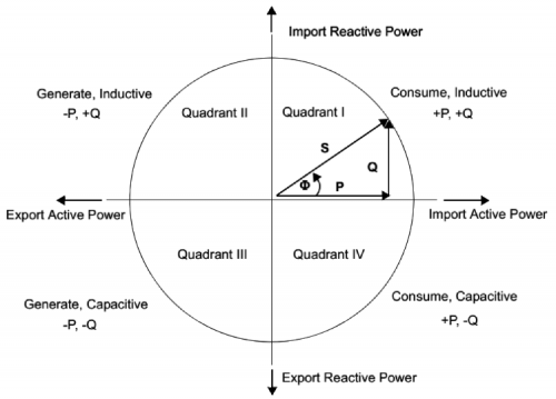
The value contained in the “ApparentPowerDivisor” register is needed in order to align the power value to the resolution set as for the values of RMS voltage and current. The measures of the real and reactive power and of the related energies may have a positive or negative sign, depending on the fact that the power (and consequently, the energy) is imported (positive sign, therefore the power is absorbed by the load) or exported (negative sign, that is to say the energy is released by the load). in the figure highlights what has just been said: please note both the power circle and the related triangle; the apparent power is indicated by the S, the reactive power by the Q. The circle is divided in quarters, so to identify if the load is of the inductive or capacitive kind, and if the energy is being imported or exported.
The accumulation of the imported/exported energy occurs at the end of every computation cycle, provided that the accumulation system has been activated; this is carried out by setting or resetting a specific bit in the “Energy Accumulation Control Register”. If this bit is reset, the accumulation system is deactivated and the accumulation registers are reset. A so-called “load” threshold must also be set; it prevents the accumulation if the power consumed by the load is below a set value.
The resolution is 0.01W; the default value loaded in the register is 100, corresponding to 1W. All the power measured under 1W will not be used in order to calculate the energy accumulation. The threshold may be set by the user, depending on the application.
The calculation of the real power is carried out as shown in the figure, where the measures of the voltage and of the instantaneous current are multiplied between them, thus originating the instantaneous power. The instantaneous power is then converted into real power by calculating the average value, or by calculating its continuous component. The real power is calculated by means of the following formula:

Please note that the equation does not have a sign, since this is given by the “Active Power Sign” bit, that is located in the “SystemStatusRegister”.

As regards the power factor, it is calculated as a ratio of the real power to the apparent power:

The value of the power factor is saved in a 16 bit register in a two’s complement, in which the most significant bit identifies the sign. The positive sign points at the fact that real power is being imported, while if the sign is negative, it means that real power is being exported. Moreover, by taking advantage of the reactive power, it is possible to understand if the load is of the inductive type (positive sign) or if it is a capacitive load (negative sign). Given that the value is represented in a two’s complement, a value such as for example 0x7FFF corresponds to a power factor equal to 1, while if the value is equal to 0x8000 the power factor is equal to -1. As regards the reactive power, it is calculated as a real power, but with the introduction of a +90° phase angle on the voltage. the figure shows the block diagram of the calculation of the reactive power. Even in this case, the register containing the value of the reactive power is devoid of the sign, since the latter is stored in the usual “SystemStatusRegister”.

The MCP39F511 registers
The registers of the MCP39F511 integrated circuit have been mapped, starting from the 0x0000 address and up to the 0x00E1 one, for a total of 225 bytes. Some registers are read-only ones, such as for example the electric measures, while other ones are for both reading and writing, such as for example the configuration registers. Depending on the function they are fitted for, the registers may be 16 bit ones (with and without the sign), 32 bit ones (with and without the sign), or 64bit ones (without the sign). The register mapping has been carried out in a coherent manner, and that means that they have been divided into categories. In other words, there are: the “Output Registers”, used in order to report the electric measures that are carried out for each computation cycle (energy accumulation registers included); the “Calibration Registers”, used in order to calibrate the measuring sections (we dealt with these registers before, when describing the measuring function blocks; as said above, they are needed in order to best optimise the available electric measurings). After that, there are the “Design Configuration Registers”, used in order to configure the integrated circuit as for its functions and to calibrate the electric measurings, with respect to the measurement target. They are followed by the “EMI Filter Compensation Registers”, that are reserved and are usually used for the nutrition monitoring applications. In order to correctly implement them, it is needed to request further support from Microchip. Finally, there are the “Temperature Compensation and Peripheral Control Registers”, that are used in order to configure some peculiar functions, such as for example the activation and the deactivation of the energy accumulation.
Communication protocol
The MCP39F511 integrated circuit uses – as a communication interface – the UART that, depending on the applications, may be opto-isolated in order to galvanically separate the high voltage part from the low voltage one. The default communication speed is 115,200kbps, and it may be modified by means of the configuration of the “SystemConfigurationRegister”. However, we advice to modify the communication speed only if it is really needed. The rest of the configuration considers 8 bit for the data, 1 bit for the start and 1 bit for the stop.
In addition to the communication interface, the integrated circuit provides a series of outputs, named as events (EVENT1 and EVENT2), that may be configured in such a way that only some significant events are reported (such as, for example, a voltage/current/power threshold being exceeded).
Another significant output (and a configurable one as well) is the ZCD (Zero-Crossing Detection) one, that returns a signal (that is coherent with the zero crossings of the sinusoidal signal found on the V+ and V- differential inputs) as an output. In the figure highlights the signal found on the ZCD pin that, as can be seen, is a square wave having a frequency that is equal to signal found on the differential inputs, but with a 200µs delay.

Another way to return this information is shown by the figure that, by means of a different configuration, sees a 100 µs output pulse for each zero crossing. Even in this case the signal has a 200 µs delay with respect to the one found on the inputs.

The communication interface enables the creation of a point-to-point connection between a host device (that could be a MCU Microchip or a PC) and a single MCP39F511 integrated circuit. The data connection from and to the integrated circuit takes advantage of a communication protocol that defines the packets according to a very specific structure, called “frame”, as pointed out by figure.

Every “frame” includes a “header byte”, followed by a byte indicating how many bytes are found in the packet. It is followed by the packet with the command (or the commands) and finally by the checksum. The maximum number of bytes for each “frame” transmitted is 35. This approach enables a solid communication, moreover no command found in the “frame” is carried out as long as the checksum and the number of bytes are not validated by the receiver.
After a “frame” has been received, the MCP39F511 integrated circuit may generate one of three possible replies:
1) Acknowledge (ACK – 0x06): the “frame” has been successfully received, the command is understood and executed
2) No Acknowledge (NAK – 0x15): the “frame” has been successfully received, but the command was not understood and therefore was not executed
3) Checksum fail (CSFAIL – 0x51): the “frame” has been successfully received, but the checksum found in the frame is wrong, therefore the packet has been discarded
The checksum is generated by adding the bytes of the “frame” received or to be sent (“header byte” included), the sum is divided by 256: the checksum is the remainder of that division.
Table 1 shows a list of the commands available for the MCP39F511; for now we will concentrate only on the first seven commands, and will omit the self-calibration ones. The command #1, coded as ID 0x4E, is needed in order to read one or more registers from the memory of the integrated circuit: we would like to remind you that it sees the mapped registers, starting from the 0x0000 address. First of all, this command needs – in order to operate – the starting address from which to start reading; in order to achieve this, it is needed to use command #3, coded as ID 0x41. At this stage we have two possibilities: the first one consists in using two different “frames”, that is to say, we send a “frame” in order to set the starting address to be read, and then we send the “frame” via the reading command. Or we may create a “frame” that contains both commands, but first we should send the command to set the pointer in memory, and then the reading command. After that, the “frame” may be set, as shown in Table 2.
table1/2


The same logic may be applied to the command #2, coded as ID 0x4D, as for the writing of the registers, starting from a given address; an example is shown in Table 3.
table3

After having written the data in the registers of interest, it is needed to send a command, in order to save the content in the Flash memory, so to maintain the setting over time. In order to do so we will use the command #4, that is coded as ID 0x53. In Table 4 the needed “frame” is detailed. The MCP39F511 integrated circuit has 512 bytes of EEPROM memory, organised as a word, and useful in order to memorise any kind of data, be it concerning the measures or other kinds of data that may be needed by the application being examined; that’s as if we had an EEPROM memory available on a SPI or I²C bus. The memory is divided in pages having 16 Bytes each (8 words) for a total of 32 pages.
table4

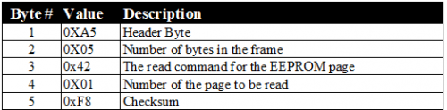
The memory is accessed at a page level; for the purpose, the integrated circuit makes three different EEPROM management commands available; a write command, a read command and a command for erasing the whole memory in one shot. Table 5 shows the details as for the reading “frame” of the EEPROM page.
On the other hand, the writing “frame” of the EEPROM page will be as detailed in Table 6.

Finally, let’s see the command for erasing the EEPROM, whose frame is the one shown in Table 7.

Calibrating the MCP39F511
The MCP39F511 integrated circuit needs to be calibrated, so to compensate the gain errors during the analog-to-digital conversions, in order to compensate the tolerance of the components used for the execution of the voltage and current measuring, and in order to enhance the noise immunity.
As hinted before, there are some self-calibration commands, that however we didn’t implement in our applications, since we preferred a manual implementation of the calibration system. Given that as for the calibration a purely resistive load must be used, the real and the reactive power will correspond.The measures requiring a calibration are obviously the RMS voltage and current, in addition to the measures for the active and the reactive power. The new value we found ranges between 25,000 and 65,535, and therefore we may consider the calibration for the current measuring as complete. If on the other hand, we wanted a 0.1mA resolution, it would mean that the value loaded in the “Calibration Current” register is no longer 1,000, but 10,000. By applying again the formula, and starting from a “Gain Current RMS” value that is equal to 33,840, we will obtain as follows:
The formula that has been used as for the calibration is:
![]()
If we look attentively at the formula, it is possible to infer that we need a reference measure (called “expected measure”), with respect to the real measure that has been carried out; for example, if the measuring of the RMS voltage is being calibrated, as a first thing we need have a stable reference voltage at the integrated circuit’s input, for example 230Vac, and then to write the voltage value expected during the calibration in the “Calibration Voltage” register. The same logic should be applied to the RMS current, in this case we should ensure to have a stable resistive load over time, so to have a reference value to work with. The registers that come into play during the calibration phase are the following ones:
- Address: 0x0060 – Gain Current RMS
- Address: 0x0062 – Gain Voltage RMS
- Address: 0x0064 – Gain Active Power
- Address: 0x0068 – Gain Reactive Power
- Address: 0x0082 – Range
- Address: 0x0086 – Calibration Current
- Address: 0x008A – Calibration Voltage
- Address: 0x008C – Calibration Active Power
- Address: 0x0090 – Calibration Reactive Power
- Address: 0x0094 – Line Frequency Reference
Let’s try with an example, and suppose we want to calibrate the measuring section of the current, by taking advantage of a calibration current equal to 1A. We impose a 1mA resolution as for current measure: this means that we have to load the 1000 value in the “Calibration Current” register; the 1000 value corresponds to the well-know “expected measure”. Let’s suppose we now read a value equal to 2,300 (that is to say, 2.3A) in the “Current RMS” register; such a value obviously exceeds the expected 1000 value, by much. Let’s apply the formula we showed you before, and supposing that “Gain Current RMS” has been set to 33,480 and that the value found in the range register – for the current measuring – is equal to 12. The achieved result is the following one:
![]()
The value that will be obtained for the gain is under the minimal allowed value, that is 25,000. Therefore we will have to modify the value found in the “Range” register. In practice, this register indicates a number of shifts to the right, that is equal to executing a division by 2, to be carried out after the multiplication with the “Gain Current RMS”, so to get closer to the measure carried out with the expected measurement. Therefore, by increasing the value in the “Range” register by 1, we will obtain the value of the measure goes from 2300 to 1150, that is a much closer value to the 1000 value, with respect to the previous situation. We will then apply the formula again:
![]()
This new value for the gain is too high, it exceeds the maximum value of 65,535; in this case we will have to act again on the “Range” register and to decrease the shift number on the right, so that the measured value is greater than before. In order to understand how many shifts to the right are to be removed, we have to divide the value we obtained as for the gain by the maximum limit of 65,535; in our case we will obtain a value of 2.2. We will pick the closest integer, that is to say 2, and consequently, the value to be set in the “Range” register will be 10 and not 12 anymore. With this new value, the current measure will be equal to 9200. By applying the formula in order to calculate the new gain, we will obtain:
![]()
The new gain is within the limits and therefore we may consider the calibration as complete.
The hardware
Well, we may consider the description of the MCP39F511 integrated circuit as complete. Therefore we may now see how it has been used in this project, that consists in two units: a plugin module that hosts the integrated circuit, and a demoboard for the plugin module, that is useful in order to start testing with the integrated circuit. The plugin board consists in a general purpose module, containing the MCP39F511, with the electronics needed for its correct functioning.

The module’s circuit diagram
Let’s start describing the circuit diagram of the plugin module, starting from the differential input for the voltage measuring. The measuring part of the module is based on two essential elements: the first one is a VT (voltage transformer), manufactured by Itacoil. In particular, that’s an SLV101201, it accepts voltage input values ranging from 100V to 275V, with a typical linear error under ±0.50%. The VT we used has two secondary windings that – depending on their connections – enable to obtain a certain output voltage.

With a nominal input voltage equal to 230V, and by connecting the secondary windings in series, a 10Veff voltage is measured at the free ends. The load resistance to be used in this case is equal to 10 kohm.
As regards the current measuring, we opted for a CT, and still, one manufactured by Itacoil, the SBT002 one, that enables a maximum nominal current of 42.5A (the maximum value allowed is 51A), with an accuracy that is the one of Class 0.2. The Burden resistance (shunt) to be used is equal to 50 ohm.

If you have to measure higher currents (but you will have to do that, to the detriment of the accuracy), you may reach up to nominal 51.6A (the maximum value allowed is 62A), but the Burden resistance value would become 5 ohm. We opted for the first solution, that is to say a nominal current of 42.5A, and therefore for a greater accuracy.
Please note that, even though they belong to the measuring circuit, both the VT and the CT are not physically located on the module but the first one is on the demoboard (that we will describe shortly), that hosts the plugin board, while the second one must be connected to the demoboard’s X2 input.

Let’s return now to the SBT002 CT (it has a 50 ohm Burden resistance): given that the input is of the differential kind, the Burden resistance is protected by using four resistors (R1, R3, R4 and R7), connected in series and giving a value of about 50 ohm. The values of R3 and R4 are thus obtained:
- IMax = 51ARMS – IMaxPeak = 72,114APeak
(Peak current on the primary) - ISecPeak = IMax / 2000 = 36,057mAPeak
(Peak current on the secondary) - Given that the maximum voltage on the differential input as for the current measuring is ±600mV, we obtain that:
– R3 + R4 = 600mV/ISecPeak = 16R64
Therefore, by dividing the value we obtained by 2, we will obtain the resistive value that R3 and R4 – that is to say, 8R32 – must take. The closest value is 8R2. By means of the difference we will obtain the value to assign to the R1 and R7 resistors:
![]()
By dividing the value we obtained by two, we will acquire the value – concerning the two resistors – that we are looking for, that is to say, 16.8 ohm. The closest value in the E96 series is 16.9 W. As regards the voltage measuring, in this case there is a VT, and we may proceed with as follows:
- Vnominal RMS = 230Veff – Vnominal P = 325.259V
(Nominal voltage on the primary) - Vnominal RMS = 10Veff – Vnominal P = 14.140V
(Nominal voltage on the secondary) - Vmaximum RMS = 300Veff – Vmaximum P = 424.264V
(Maximum voltage on the primary) - Vmaximum RMS = 13.043Veff – Vmaximum P = 18.443V
(Maximum voltage on the secondary)
Therefore, given the peak voltage on the secondary – that is equal to 18.443V – we may acquire the values that the voltage divider’s resistors at the differential input of the integrated circuit must take. Given a value that is equal to 1 kohm as for R11, we may calculate Rx:
![]()
![]()
From all of this it turns out that the R8, R9 and R10 resistors may take the following resistive values: 27 kohm, 2K2 and 560 ohm. Given that AN_IN is not being used, we connected it to ground by means of a 1,000 ohm resistor.
All the analog part we just described has its (analog) ground that is connected to the digital ground of the PCB via a jumper (0 ohm resistor).
The two grounds are thus connected in a single point, preventing that the digital section may “contaminate” the analog part, thus compromising the electrical measures. Given that the board is born as an item to be added to your own projects, a connector The module has a connector for the purpose.. of bringing the analog signals coming from the VT and from the CT, in addition to a connector for the digital interconnections towards a microcontroller or something else. Our connector is therefore composed of the CN2 and of the CN3. CN2 concerns the purely analog part, while CN3 deals with the digital connections. In particular, we returned the TX and RX signals of the UART interface, the ZCD (Zero Cross Detection) signal, the MCLR and RESET signals, including the pull-up resistor. Please note that no opto-isolation has been prepared, since the usage of a VT and of a CT as for the electric measurings ensures a galvanic isolation from the network’s voltage. If we had opted for a simple resistive voltage divider, starting from the network voltage, and for a resistive shung for the current measuring, it would have been needed to use opto-isolators. In order to parametrise the MCP39F511 integrated circuit, specially during the calibration, we thought to add the CN1 connector, to which the RS232/USB FT782M converter may be connected.
The connector simply considers the RX and TX signals of the UART, in addition to the +5V and the GND power source. Given that the MCP39F511 integrated circuit has a 3.3V power source, a MCP1801T-3302I/OT voltage regulator has been added, in order to generate the needed voltage of +3.3V. In order to disable the voltage regulator, it is enough to move the J1 jumper to the position 2-3, while if you wish to use the voltage regulator, the J1 jumper must be set to 1-2. The MCP1801 integrated circuit is a LDO (a low-dropout regulator, having a typical drop-out of 200mV at 100mA), capable of supplying an output current up to a maximum of 150mA, which is enough for most applications involving a microcontroller. Both on the input section and on the output one, it is enough to place some 10µF/16V ceramic capacitors. Finally, we prepared three LEDs: the LD1 green LED is connected to the EVT1 (EVENT1) line, while the LD2 yellow LED is connected to the EVT2 (EVENT2) line, therefore depending on how the MCP39F511 integrated circuit is programmed, we will return some pieces of information concerning the events occurred during the functioning (for example, a power threshold is exceeded, or something else) on the said LEDs. Finally, the LD3 red LED indicates that the power source was found. In the case in which you decided to manually assemble the components on the said board, please always start from the MCP39F511 (U2) integrated circuit, that is the most critical component to solder, since it exists only in the 28pin QFN 5×5 case.
Please use much flux and a hot air solder. Later, you will be able to move on to the U1 voltage regulator and finally to the resistors and to the 0603 capacitors. Lastly, please mount the interconnectors. Before powering the board, please accurately check that all the solderings have been properly carried out and that no short circuit is found.
The energy meter demoboard
As a first application, we propose a very simple project, that will immediately allow you to use our measuring board. The project also considers a board calibration/programming software, in addition to the possibility to read and save the electric measures executed by the measuring board. The demoboard’s circuit diagram is a very simple one and it has two 90° extractable terminal blocks, X1 and X2, for the 230V network voltage connection and the CT converter, in addition to two connectors, CN1 and CN2, for the connection of the USB/RS232 FT782M converter that is needed in order to interface our measuring board to the PC. The CN1 connector enables a vertical insertion, while CN2 enables an horizontal connection. The X1 terminal block brings the 230V network voltage to the VT transformer for measuring the electrical quantities: that’s the SVL101201 one, manufactured by Itacoil, that we previously discussed.

The galvanically isolated output signal is brought to the MCP39F511 measuring board. In this project we used the vertical insertion board, that is to say, the MCP39F511_BOV. The X2 terminal block brings the signal of the Itacoil SBT002 CT to our measuring board, and even in this case we are galvanically isolated from the 230V network. Out of the digital output signals from the measuring board, in this case we are only interested in the TX and RX lines of the UART, to be brought to the USB/RS232 FT782M converter. The +5V power directly arrives from the USB connection and is brought to the MCP39F511_BOV board. The board’s PCB has been designed for the purpose of being inserted in the Teko Coffer 2.5 case, once it has been opportunely milled for the housing of the two extractable terminal blocks, X1 and X2, and of the mini-usb connector, either on the right side of the box or on its lid, depending on the fact that the converter is mounted vertically or horizontally.
In order to mount the components on the board, we advise to start from the R1 resistor, followed by the CN1 and CN2 connectors, and then by the X1 and X2 terminal blocks, by the MCP39F511_BOV measuring board (we advise you to solder it directly to the board) and finally the VT transformer by Itacoil.
In this way, the board is ready to be inserted in Teko’s case. Please use the dedicated spacers, in order to prevent the board from touching the back of the box. We used some D/3000 spacers by SC.
Conclusions
In this first installment we presented the integrated circuit at the basis of the Energy Meter, and the demoboard to use it.
In the next installment it will be followed by the description of a software, designed for the purpose of the programming/calibration of the MCP39F511, and by the displaying of the electrical measures carried out, so to have a graphical feedback that may be easily understood.
Components List:
C1, C6, C11: 100 nF (0603) ceramic capacitors
C2, C3, C4, C12: 10 µF (0603) ceramic capacitors
C5: 1 µF (0603) ceramic capacitor
C7÷C10: 33 nF (0603) ceramic capacitors
R1, R7: 16,9 ohm 1% (0603)
R2: 10 ohm 1% (0603)
R3, R4: 8,2 ohm 1% (0603)
R5, R6, R11÷R14: 1 kohm 1% (0603)
R8: 27 kohm 1% (0603)
R9: 2,2 kohm 1% (0603)
R10: 560 ohm 1% (0603)
R15÷R17: 1,2 kohm 1% (0603)
R18: 0 ohm (0603)
R19, R20: 10 kohm 1% (0603)
L1, L2: Ferrite (0603)
LD1: green LED (0603)
LD2: yellow LED (0603)
LD3: red LED (0603)
U1: MCP1801T-3302I/OT
U2: MCP39F511-E/MQ
Other information:
– 4-way female strip splitter
– 3-way male strip splitter
– 4-way 90° male strip splitter
– 10-way 90° male strip splitter
– Jumper
– S1346 printed circuit board
Components List:
R1: 10 kohm
U1: MCP39F511 (FT1346) module
TF1: SVL101201 transformer
Other information:
– 2-way extractable terminal block (2 pcs.)
– 4-way 90° female strip splitter
– 4-way female strip splitter (2 pcs.)
– 10-way female strip splitter
– S1348 printed circuit board
From openstore
CURRENT MEASUREMENT TRANSFORMER
VOLTAGE MEASUREMENT TRANSFORMER

[…] can do all of that, but needs a little help from a few transformers. [Boris Landoni] has a two-part post that not only shows such a meter built with the chip but also has a very detailed description of […]
[…] Energy Meter module to analyze the electrical grid parameters and consumption (part 1)Posted 1 month ago […]
[…] can do all of that, but needs a little help from a few transformers. [Boris Landoni] has a two-part post that not only shows such a meter built with the chip but also has a very detailed description of […]