
It enables a selective disconnection of a maximum of 7 users, once the maximum power set is exceeded, and by selecting the priorities, so to disconnect the less important ones first.
Supervising the electricity, intended as both the monitoring and the management and even as a possible limitation and optimisation, is a topical issue since a few years, and above all since energy supply has become a relevant problem; it is not a case that since a while a belief has arisen: that we should save energy, rather than be looking for miracle energy sources. Laws and cutting-edge technologies enable now the existence of devices that comply with some pressing consumption limits, and especially when in idle mode. It is under this perspective that we have to see the Energy Meter project, that has been published in the previous post: part1 and part2; it enables the measuring – thanks to the MCP39F511 integrated circuit – of the real, reactive and apparent power, of the RMS values as for voltage and current, of the network frequency, of the power factor and of the active/reactive imported/exported energy.
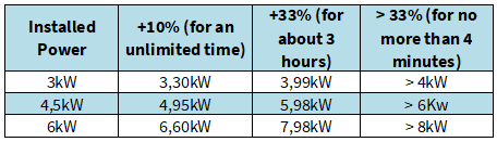
When supplying houses or small offices and shops, that are single-phase ones, the electric powers that have been installed range from a minimum of 3kW to a maximum of 6kW, with an intermediate value of 4.5kW. All the electric meters that are installed in our houses are of the electronic kind, and this is true both for the old generation ones (starting from 2001) and for the second generation ones, that will substitute the ones that are currently being used.
An electronic meter enables to exceed forever the 10% of the installed power. In other words, if your energy supply contract considers an installed power of 3kW, it is always possible to draw a power equal to 3.3kW, for an unlimited time, without ever having the power cut because of an excessive absorption.
The electronic meter also considers a second tier for the power output, that enables to absorb a maximum power that is about 33% greater with respect to the available one, for not more than three hours.
Let’s return to our example: the maximum supplied power for about three hours is equal to 3.99kW; once the 33% threshold has been exceeded, the electric meter comes into action within 4 minutes, and it cuts the power.
In Table 1, the situation is summarized as for the different cases in which the power is cut.
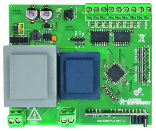
There are some systems, that are available for sale, for the purpose of disconnecting the non-primary lines; they may manage a single line to which all the loads that may be disconnected from the network in the case of an overload are connected; in these pages, you will find our version. The system is based on the measurings that have been carried out via our FT1346M board, to be paired to the SVL101201 VT and to the SBT002 CT.
Table 1
The firmware loaded in the microcontroller also enables to run what follows:
1) adjustment of the LCD contrast;
2) configuration of the installed power (default value 3kW);
3) adjustment of the TOFF time. The TOFF time identifies the period of time the non-primary line has to remain disconnected, before it may be rearmed; the default value is 4 minutes;
4) the possibility to have a forcibly ON non-primary line; therefore, in the case the threshold is exceeded, the power to such a line won’t be cut;
5) the possibility to test the non-primary lines;
6) the possibility to reset the electric meters;
7) the displaying of the following electrical measures:
- RMS voltage and current;
- apparent, real and reactive power;
- power factor;
- line frequency;
- real and reactive imported power;
- real and reactive exported power;
- the situation concerning the non-primary lines: activated, disconnected or forcibly ON line.
Each time the set threshold has been exceeded, the system will deal with disconnecting the non-primary lines in sequence, and for the purpose of showing this, the LCD display will start flashing.
HOW IT WORKS
Let’s see now the functioning of the system as for the disconnecting the non-primary lines; we will do that with reference to Fig. 1: what is shown is a graphic representation of the trend of the power for a possible electrical system having a 3kW electric meter. Two thresholds, that we previously referred to, are pointed out in the figure: the first one corresponds to the installed power adding +10%, that as for the example shown is equal to 3.3kW (the dashed blue line), while the second one is equal to the installed power adding +33%, that is to say, 3.99kW (the finely dashed red line).
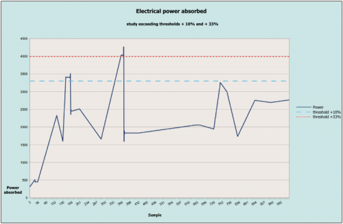
Fig. 1
Now, what we wish to do is that – when the absorbed power exceeds the blue threshold for more than two seconds – the system automatically disconnects the first non-primary load, and then tries to rearm it as soon as possible, provided that the conditions allow it. If on the other hand, the absorbed power exceeds the second power threshold (the red dashed line), the system has to promptly come into action and to disconnect the first non-primary load, within 200ms.
Please remember that when the absorbed power exceeds the second threshold, there is a maximum of four minutes before the intervention; thanks to such an approach it is ensured that it never has to wait for more than 4 minutes. In both the cases we just explained, the system will try to rearm the line as soon as possible, or after a period of time set by the user, and if the instantaneous absorbed power is such to allow to rearm the line of interest, without having the threshold to be exceeded again.
The system we developed is capable of managing up to a maximum of seven different lines, with line 1 being the one having the lowest priority, while line 7 is the one with the highest priority; this means that the disconnection of the non primary lines will start from line 1 and all the way to line 7. The rearming will occur precisely in the opposite direction: starting from line 7 and all the way up to line 1, still provided that the conditions allow it.
CIRCUIT DIAGRAM
The block diagram shown in Fig. 2 defines the architecture on which we operated for the development of the electronics needed for the purpose of cutting the power of the non primary lines; the whole has been divided into two boards: a foundation one and another one that is applied upon the first one, and that contains the display and the buttons (the user interface).

Fig. 2
The “electronic brain” of the system is found on the foundation board and that’s the PIC18F46K22 microcontroller: it manages both the part concerning the configuration and the display of the electrical measures and the part concerning the measuring and the disconnection of the non-primary lines. Therefore, and starting from the measuring section, there is our FT1346M board (U3, that was already described when dealing with the Energy Meter project), equipped with the MCP39F511 integrated circuit, to which two measuring transformers are connected; they are the VT and the CT, that are respectively destined to the measuring of the voltage and of the current.
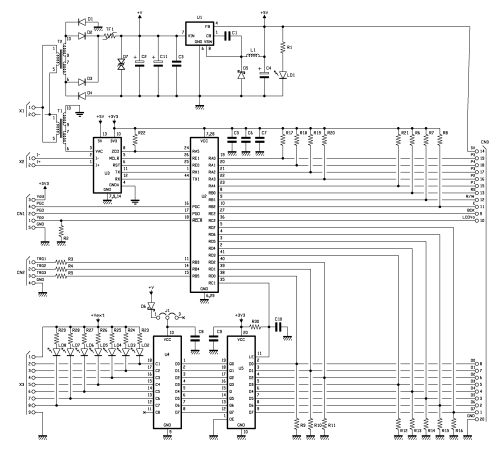
The FT1346M communicates with the microcontroller via the UART serial interface; on the other hand, the 8 bit data bus communicates both with the alphanumeric LCD display with two lines (for a total of 16 characters), and with the section for the management of the open-collector outputs (for the management of the non primary lines). In addition to the LCD display, we arranged the five buttons (so to allow you to interact with the system) on the user interface board.
Finally, there is the power source section, that is composed of a line transformer, and a switching voltage regulator for the generation of +5Vcc needed by the board.
After this premise, we may move on to the detailed description of the circuit diagrams, since the electronics is divided into two different PCBs: the first one, named as the “foundation” one, on which the greatest part of the electronics is hosted; and the second one (front board) on which there are the buttons and the LCD display. The two boards are interconnected via a dedicated pin-strip.
Foundation board
Let’s start with the foundation board and describe the power source section; Fig. 3 shows the function blocks in which it is possible to divide our power source section, that is to say: the flyback transformer, the diode bridge, the level capacitors and the voltage regulator. The power for the relays is drawn upstream of the voltage regulator.
The T2 transformer draws two 9Vca voltages from the network’s 230Vca; the secondary windings are connected in series, so to ensure an 18Vca nominal voltage and a 0.333A maximum current. The usual diode bridge follows, downstream of it there is the PTC protection fuse in the TF1 current and the TVS diode that protects from overvoltages, and then the level capacitors. The self-resettable protection fuse (PTC) ensures a 500mA holding current, that is more than enough for our application, and comes into action if the absorption on the part of the following circuit exceeds 1A. Once this has been reached, the device opens. The TF1 thermal fuse operates in pairing with the SM6T33CA transit diode, that has a nominal breakdown voltage that is equal to 33V and a 45.7V clamping voltage: as long as the voltage at the ends is under 30V, the transit diode virtually absorbs nothing, while if it goes up, for example, because of a 230Vca overvoltage on the network, the component has a growing absorption with the voltage increasing; a short circuit occurs when the voltage exceeds the clamping one. The maximum power dissipation that the transit diode withstands is 600W, therefore it is capable of managing pulse overvoltages in the range of ±500V. The fact that there is the TF1 thermal fuse makes it so that the circuit is interrupted when the transit comes into action.
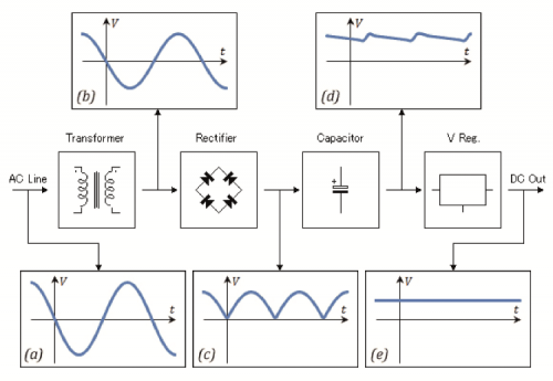
Fig. 3
Let’s go now to the voltage regulator that enables to obtain stabilized +5Vcc: that’s an LM2675 switching one, that is capable of supplying a maximum current of 1A: that’s more than enough for our application. The maximum efficiency that the voltage regulator may reach is 96%, with a working frequency that is equal to 260 kHz. The input section accepts voltages ranging from a minimum of 8Vcc and up to a maximum of 40Vcc, and therefore that’s perfectly compatible with our electronics.
The green LD1 LED deals with indicating that the +5Vcc voltage is found on the board; the +5Vcc power voltage is brought both to the FT1346M board (that generates the +3.3Vcc power voltage) and to the front PCB, by means of the connection flat cable.
The heart of the system is the PIC18F46K22 microcontroller that – thanks to its 64 kByte Flash memory (32768 Single-Word Instructions), to the 3,896 byte SRAM memory, to a 1024 Byte EEPROM and to a processing speed of 16 MIPS – has everything needed in order to develop the firmware needed for the management of all the peripherals interconnected to it.
The communication towards the MCP39F511 integrated circuit – found on the FT1346M board – is carried out by taking advantage of the UART1 (TX1 and RX1) peripheral, that operates at 115200Baud, with 8-bit data, no parity and one stop bit, as required as per default settings by the integrated circuit itself. In addition to the TX1 and RX1 lines, the MCLR, RESET and ZCD lines are needed. The first two lines are respectively needed in order to keep the whole integrated circuit in the reset state, while the second one keeps only the ADC converters, the PGA amplifiers and the other function blocks of the analog front-end in the reset state. On the other hand, the ZCD line is needed in order to monitor the zero crossings of the network sinusoid (ZCD = Zero Cross Detection) on the part of the PIC. In practice, the microcontroller is capable of understanding if there is a network voltage or not at the 230Vac inputs. As for the measuring of the voltage quantities, the Itacoil SVL101201 (T1) VT is used, with its secondary windings connected in series, so to obtain a 10Vac nominal voltage when on the VT’s primary there is a 230Vac voltage. The voltage range allowed on the primary goes from 0Vac up to a maximum of 300Vca (on the other hand, the precision range goes from 100V to 275Vca).

Therefore, it may be summarized as follows:
Vnominal RMS = 230Veff –> Vnominal P = 325.259V (nominal voltage on the primary)
Vnominal RMS = 10Veff –> Vnominal P = 14.140V (nominal voltage on the secondary)
Vmaximum RMS = 300Veff –> Vmaximum P = 424.264V (maximum voltage on the primary)
Vmaximum RMS = 13,043Veff –> Vmaximum P = 18.443V (maximum voltage on the secondary)
These values are compatible with the electronic parts found on the measuring board. The terminal block – as for the connection of the 230Vac network voltage – is X1.
The SBT002 CT by Itacoil enables the measuring of a maximum current that is equal to 51A, thanks to its 2000 sec turns. Therefore, the allowed values are:
IMax = 51ARMS –> IMaxPeak = 72.114APeak (peak current on the primary)
ISecPeak = IMax / 2000 = 36.057mAPeak (peak current on the secondary)
These values are compatible with the electronic parts found on the measuring board. The CT must be connected to the X2 terminal block.
The PIC’s D port is used as an 8-bit data bus, to which both the LCD display (found on the front board) and the latch (the one used in order to drive the U4 Darlington array) are connected. The pull-down resistors – the ones that ensure that the lines are kept at a low logic state, in the case in which the PIC has not been programmed or when – for some other reasons – the D port’s lines go at a high impedance – are connected to the data bus.
The U5 latch considers two control pins, named as OE and LE. The first one is known as a 3-state output enable, it is active at a low level and is needed in order to remove the high impedance condition from the latch outputs. Given that the output lines are only connected to the U4 integrated circuit, it is possible to connect the OE signal directly to GND, without worries. The LE line, on the other hand, is needed in order to “freeze” the state found on the data bus and therefore to transfer it to the outputs of the Latch. The line is active at a high level, therefore it is normally kept low, as long as the piece of data found on the bus has not to be transferred to the outputs of the latch. We also added a pull-up resistor and a filter capacitor in order to prevent spurious activations.

On the outputs of the U4 integrated circuit, there is a transistor array in the Darlington configuration, to which to connect the coils of the relays to be driven.
We supplied a LED for each line, so to see when the line is active (therefore, when the relay is excited), and when the line is turned off (therefore, when the relay is not excited). The U4 integrated circuit also contains the recirculation diodes, to be arranged in parallel to the relay’s coils. We would like to point out that the system is capable of driving up to a maximum of 7 independent non-primary lines. Given that the data bus is an 8 bit one, there will be a free line, and in particular, the pin 11, signed as C8. The power voltage of the coils may be drawn directly from the PCB, by inserting the J1 jumper in the 1-2 position, therefore that’s for relays with a 24Vcc coil voltage. If on the other hand, you wish to power the coils of the relays via an external voltage, you will have to place the jumper on the 2-3 position. If you use an external power source, it has to be compatible with the power voltages of the coils of the relays that have been used.
Please pay attention to the coil voltage of the relays that have been used, since if it is a low one – for example, 12Vcc – the current needed in order to drive the coil of the relays will increase.
The other way around, if the coil voltage is equal or greater than 24Vcc, the needed current will decrease.
As regards our application, we used some Finder relays of the 40.61.7.024.4001 series; they have a nominal coil voltage that is equal to 24Vcc (the minimum allowed value is 17.5Vcc; the maximum allowed value is 36cc). The excitation current is 21mA (we are using a sensitive, 0.5W version). The standard version requires 27mA, therefore that means that when all the seven relays are excited, the current needed will be about 147mA. Let’s return to the previous discussion: if we had opted for a relay having a 12V coil voltage (40.61.7.012.4001), then the current needed in order to drive the coil would have been 42mA, for a total of 294mA. Vice versa, with a relay having a 48V coil voltage (40.61.7.048.4001), the current needed would have been 10mA, for a total of 70mA. That being said, if you wish to use some relays that are different from the ones we used, please pay attention to these nominal values as for voltage and current.
But above all, please remember that our electronics have been designed for relays having a 24Vcc coil voltage, therefore if you use different relays, you will have to supply some adequate power to the coils, and then to move the J1 jumper to the 2-3 position.
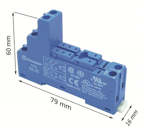
Fig. 4
Given that the relays of the 40.61.7.024.4001 series were born in order to be mounted on the printed circuit board, while we need to mount them on a DIN rail for an electric panel, it is needed to acquire some dedicated Finder sockets. In particular, we need those of the 95.05 series (terminal box clamp socket, mounting to panel or 35 mm rail), as shown by the example in Fig. 4. If you so prefer, there are some relays for a DIN rail, still manufactured by Finder: they are of the 22.21.9.024.4000 type, with a 24Vcc coil absorbing a 52.2mA current. Our electronics are not capable of supplying a current of about 365mA in order to drive 7 relays such as these ones. In this case, it would then be possible to opt for an external power source, as indicated above, or to use a maximum of 4 relays with our electronics, thus leaving 3 lines free. We would like to point out that it is not mandatory to use all the seven available lines; the user is free to use as many as he wishes; what is really important is that you start wiring the electric system from the line 1, until you reach line 7. The 78.12.1.230.2400 (by Finder, as per model is shown in Fig. 5) or the DSP10-24 (TDK-Lambda) could be a possible external power source for an electric panel that would be capable of supplying the current needed in order to drive the 22.21.9.024.4000 Finder relays.
Obviously, the power source becomes mandatory in the case in which you wish to use all the open-collector outputs for the management of the non-primary lines, otherwise, it is not strictly needed and it only adds a cost.
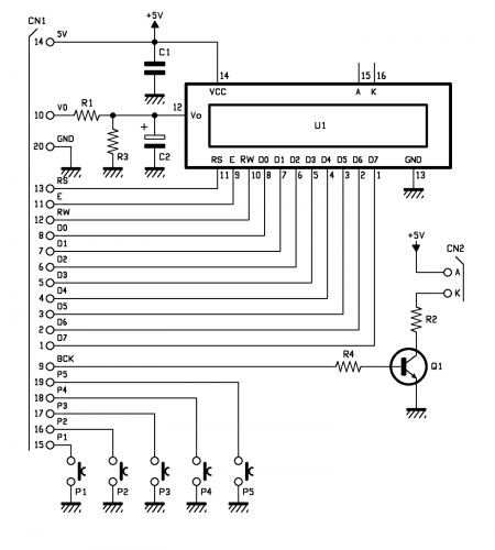
Let’s continue now with the description of the circuit diagram: the data bus is brought to the LCD screen as well, and therefore to the CN3 connector, that is composed of two 10-pole terminal strips. In addition to the data bus, the BCK, LCD_V0, E, R/W and RS lines are brought to this connector. The BCK line is needed in order to turn on and off the backlight of the LCD screen, the LCD_V0, is needed to adjust the LCD contrast, by means of a PWM signal, the E line is the chip enable signal, and it informs the display’s electronics that the data passing through the bus concern the LCD screen, the R/W line is needed to inform the display that a reading or writing command is being executed, while the RS line is needed in order to inform the display whether we are sending a command or data.

Fig. 4
On the CN3 connector, there are the lines for the buttons from P1 to P5, they are needed in order to manage the functions that are made available by the device.
Some pull-up resistors have also been added for the E, R/W and RS lines, as well as for the lines of the buttons from P1 to P5.
As regards the firmware debugging, three trigger lines, named as TRG1, TRG2 and TRG3, have been arranged. They are brought to the CN2 connector by means of a series protection resistor.
The CN1 connector is needed for the in-circuit programming of the microcontroller, as well as for the development stage and for the firmware debugging. In fact, it is possible to connect the development systems by Microchip (such as ICD3, ICD4 or RealIce) to this connector.
User interface diagram
The front board, whose circuit diagram may be seen in these pages, includes the LCD screen of the 162D series by Displaytech, the five buttons and some other side components.
The communication interface of the LCD screen includes the 8-bit data bus, in addition to the three control lines, as already mentioned. Fig. 6 shows the line temporizations for a writing session. As a first thing, the piece of data on the 8 bit bus is set, and still keeping in mind that there must not be active enable lines, otherwise the piece of data may be acquired even by another integrated circuit that is not interested in it; at a later time the RS and R/W lines are moved, so to inform whether a piece of data (RS at a high logic level) or a command (RS at a low logic level) is being sent.
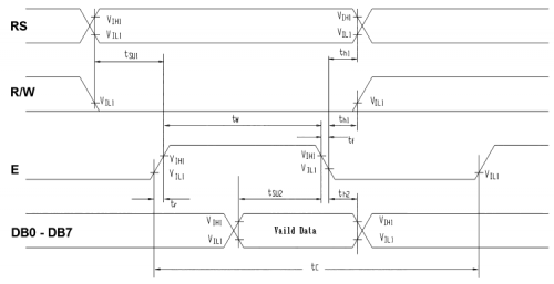
Fig. 6
Given that this is a writing session, the R/W line must be at a low logic level. Finally, after at least 40 ns, the E line must be brought to the high logic level, so that the piece of data found on the data bus may be transferred to the logic that is internal to the LCD screen. The E line must be kept at a high level for a period of time of at least 220nSec, before it may be brought at a low level again. Fig. 7 shows the line temporizations for a reading session. The same remarks we made for the writing session are still valid, with the exception of the fact that the R/W line must be at a high logic level.
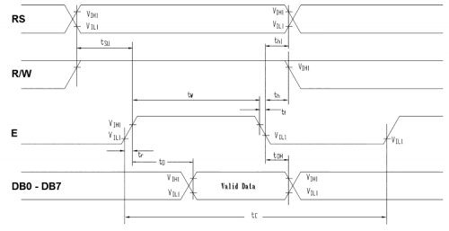
Fig. 7
The display’s electronics is completed by the R1, R2 resistors and by the C2 capacitor; they are used in order to adjust the LCD contrast, by means of a PWM signal that is generated by the microcontroller. In order to turn on and off the display backlight, we will have to act on the pins 15 and 16, that respectively identify the anode and the cathode. In order to do so, we simply inserted a transistor (Q1) that operates as a switch. Finally, there are the five buttons, P1÷P5. As with the foundation board, all the lines refer to a connector (in this case that’s CN1), to which the connection terminal strips are connected.
Components List:
C1: 10 nF (0603) ceramic capacitor
C2: 220 µF 50 VL electrolytic capacitor (F)
C3, C5: 100 nF (0603) ceramic capacitors
C4: 10 µF 25 VL tantalum capacitor (B)
C6: 10 µF 25 VL (0603) ceramic capacitor
C7÷C9: 100 nF (0603) ceramic capacitors
C10: 220 pF (0603) ceramic capacitor
C11: 220 µF 50 VL electrolytic capacitor (F)
R1: 4,7 kohm 1% (0603)
R2: 4,7 kohm 1% (0603)
R3: 1 kohm 1% (0603)
R4: 1 kohm 1% (0603)
R5: 1 kohm 1% (0603)
R6÷R21, R30: 4,7 kohm 1% (0603)
R22÷R29: 10 kohm 1% (0603)
LD1: green LED (0805)
LD2÷LD8: red LEDs (0805)
D1: S1M
D2: S1M
D3: S1M
D4: S1M
D5: SS16-E3/61T
D6: SS16-E3/61T
D7: SM6T33CA
L1: 47µH/600mA Inductor
U1: LM2675M-5.0/NOPB
U2: PIC18F46K22-I/PT (MF1371)
U3: FT1346M Module
U4: ULN2803ADW
U5: SN74HC573ADWR
T1: SVL101201
T2: 9V + 9V Transformer
TF1: PFRA050
Other information:
– 10-way FSN22A flat ribbon cable (2 pcs.)
– 3-way male strip-splitter
– 4-way male strip-splitter
– 5-way female strip-splitter
– Jumper
– 2-way 5.08mm terminal block (2 pcs.)
– 8-way 5.08mm terminal block
– S1371 (103 x 86 mm) printed circuit board
From openstore
CURRENT MEASUREMENT TRANSFORMER
VOLTAGE MEASUREMENT TRANSFORMER

Where can I get this system ?
https://store.open-electronics.org/Energy-meter-module-ft1346m