
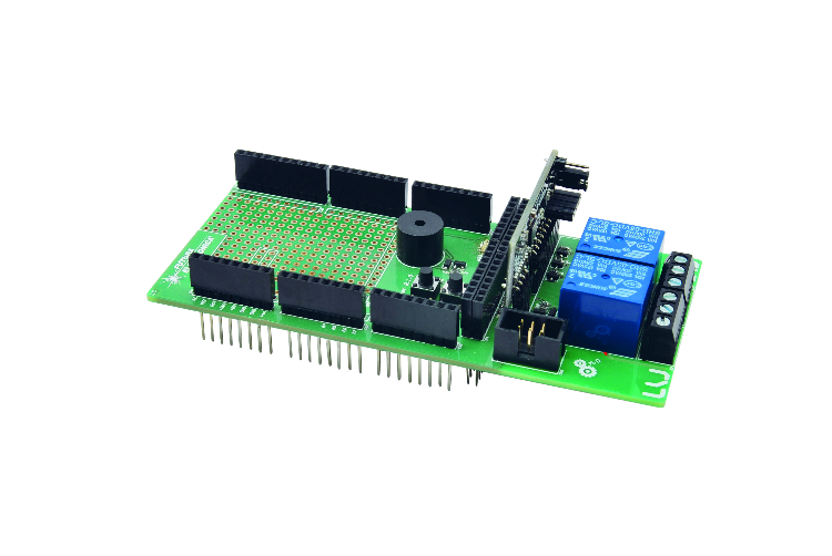
It monitors electricity consumption and sends the detected data to the cloud through the GSM cellular network; it is based on an Arduino Mega equipped with GSM Shield and an absorption detector board. First instalment.
Monitoring the electricity consumption of your home or business is an increasingly topical issue. The electrical measurements made, grouped in a database and then shown in graphical form, allow you to assess the consumption trend over time. That’s why, using our “energy meter” board FT1346M (based on MCP39F511 and presented in the previous post) we will propose a series of articles in which we are going to develop a measurement system based, first, on Arduino boards and then on other architectures. This will be combined with the new GSM Shield to add a mobile data connection and send the acquired measurements to a remote server. In the project described in these pages, we will use the Arduino Mega 2560 (or Fishino Mega), which will “run” a sketch integrating the management library of the MCP39F511 and dedicated hardware for the interconnection of the FT1346M board. The hardware we developed has the following features:
- Data connection to the FT1346M board via UART 3 hardware interface (I/O 14 and 15);
- MCLR and RESET control lines connection to FT1346M board (I/O 46 and 45);
- ZCD (Zero Cross Detection) line connection to FT1346M board (I/O A12 or 20);
- TA and TV connection to the FT1346M board (TA and TV are mounted on an auxiliary board);
- jumper to select connection of ZCD line to Arduino board; connection to I/O A12 for management through PCINT20 peripheral or to I/O 20 through INT1 peripheral;
- two independent relays for the management of any loads;
- buzzer for acoustic signals depending on operating conditions;
- four LEDs, plus two general-purpose buttons.
The PCB provides a small prototyping area where any THT component test circuits can be mounted to test specific applications. Given this simple premise, let’s move on to the description of both the block diagram and the wiring diagram.
HARDWARE BLOCK DIAGRAM
Fig. 1 shows the composition of the system: the board presented here is designed to be combined with our GSM development board (cod. WWGSMSHIELD) and consequently connected to an Arduino Mega 2560 or Fishino Mega board.
The power supply to the board can come directly from the Arduino Mega, passing through the GSM shield via micro-USB cable, or using the FT782M converter used for the AT commands sent to the GSM module.
The EnergyMeter shield can also be used without the GSM board.

Fig. 1
SHIELD WIRING DIAGRAM
As you can see, the wiring diagram is straightforward. We start by connecting the FT1346M measurement board to the Arduino Mega 2560 board, for which we have provided a level adapter between the signals, which are 0/5V for the Arduino Mega and 0/3.3V for the FT1346M. The task is performed by BSS123 MOSFETs. Let’s briefly review the concept by analyzing the TXD3 line, i.e., Arduino to MCP39F511. If the TXD3 line on the +5V side is at the high logic level, then it will also be at the high logic level on the +3.3V side since the internal diode of the MOSFET is interdicted and the channel of the MOSFET is open. When you bring the line low on the +5V side, the internal diode goes into conduction, bringing the logic state low on the +3.3V side as well. This causes the VGS to exceed the threshold by triggering the MOSFET. The same concept applies to the RX line with the difference that the signal travels from the MCP39F511 to the Arduino. We have used this connection for TX and RX lines of UART3 (I/O 14 and 15, respectively) and the ZCD line (connected to I/O A12 if PCINT20 peripheral is used or connected to I/O 20 if INT1 peripheral is used). The selection is made by jumper J1; if in position 1-2 GPIO 20, if in position 2-3 GPIO A12.
On the other hand, we opted for a simpler voltage divider for the MCLR and RST lines (connected to I/O 46 and 45, respectively). The RST line keeps the delta-sigma analog-to-digital converter, PGA amplifier, internal VREF, and other front-end analog sections in reset. Instead, the MCLR line is used to keep the entire electronics of the device reset.
The board has two general-purpose pushbuttons (P1 and P2) connected to I/O 42 and 43; the rest of the pushbuttons, i.e., not pressed, is the high logic level (+5V) maintained by two pull-up resistors. When a button is pressed, logical zero is forced to the input. Using special routines, the state is tested, and debouncing is performed: the state is considered valid if it remains for at least 50 ms.
A buzzer for acoustic signals is connected to I/O line 44, while the two relays for load management are connected to I/O lines 22 and 23. Finally, we have arranged for four general-purpose LEDs connected to I/O lines 24, 25, 26, and 27, respectively.

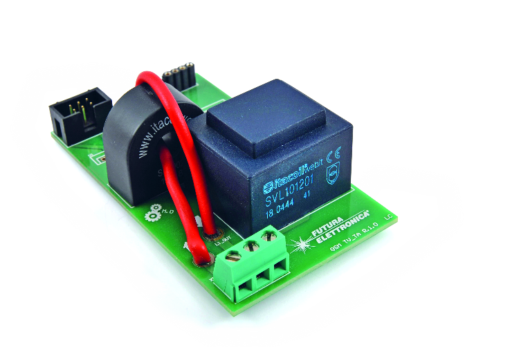
ELECTRICAL DIAGRAM TA-TV BOARD
In addition to these electronics, we have a second circuit where the CT and the TV are mounted and, through a special connector, the signals are brought to the shield and then to the FT1346M. The wiring diagram shows the TA SBT002 and the TV SVL101201, both from Itacoil. The analog measurement signals are taken to the CN2 connector; the CN1 connector, for connection to the USB/Serial FT782M interface, and the FT1346M measurement board are prepared but not mounted (the hardware is designed to be used independently, in other words by mounting the measurement board and the USB interface you have a measurement system to be connected directly to the PC and thanks to the software EnergyMeter R.1.0.4.0 or higher you can monitor the electrical measurements). This electronic is designed to be inserted in the modular container for DIN bar Italtronic 05.0302530 (H53).

MCP39F511 Arduino Library
Now, let’s talk about the library specifically developed for Arduino boards and used in the presentation sketch. The C/C++ code of the library has been divided into several files to facilitate understanding and to group the various functions developed in distinct categories such as:
- I/O management functions;
- interrupt management functions;
- serial communication management functions;
- Integrated MCP39F511 register read/write management functions.
Then the following files with .cpp extension and related .h files were created:
- “Io_MCP39F511.cpp” file and related .h file;
- “Isr_MCP39F511.cpp” file and related .h file;
- “Uart_MCP39F511.cpp” file and related .h file;
- “Cmd_MCP39F511.cpp” file and related .h file;
- “Typedef_MCP39F511.h” file containing the typedef associations used in the code for fundamental types like int8_t, uint16_t etc. Typedefs are also defined in the “Cmd_MCP39F511.h” file, but they refer to some configuration/state registers of the integrated circuit.
We start the library description from the “Io_MCP39F511.cpp” file and its .h file containing the definitions of the I/O pins used and the declarations of variables and functions for their management. Let’s start from the .h file that at the top, you find the possibility to choose which Arduino board you want to use, which is Arduino Uno R3 or Arduino Mega 2560 (Fishino Mega). As usual, we use the directive to the compiler #define followed by a string. To select the desired tab, simply remove the “//” characters from the beginning of the line, de-commenting it; only one tab can be selected at a time.
Next is the section for selecting the UART interface you want to use; in our case, we selected UART3 in hardware. Depending on the hardware you are going to use and therefore depending on where you decided to connect the UART of the MCP39F511, you will select the desired UART. If you choose to use software UARTs, you must be careful because it is difficult to go beyond 19200 Baud on Arduino boards. So, since MCP39F511 is factory set at 115200 Baud, you will first have to set it to work at the speed of 19200. This configuration can be done using the EnergyMeter software that we have already presented on the magazine’s pages. We will talk about it later since a new version has been developed with additional functions compared to the previous one.
Once the communication interface has been selected, you must decide which interrupt peripheral you want to use to manage the ZCD (Zero Cross Detection) line. Using the available hardware, we can choose to use either the external interrupt INT1 or the external interrupt PCINT20 (select hardware connection via jumper).
Again, only one peripheral can be used/selected. Remember that if you choose the INT1 peripheral interrupt, you lose the ability to use the I2C interface (this is for the Arduino Mega 2560 board, on the Arduino Uno R3, the INT1 peripheral is mapped elsewhere), while if you select the PCINT20 peripheral interrupt, you cannot use the software UART because the port change interrupt vectors would already be assigned to the Software UART library.
The I/O pin definitions of the RST, MCLR and ZCD lines follow. These associations are calibrated to our hardware but can be modified as desired depending on the hardware you are using/designing. As you can see, there are two possible configurations: one inherent to the Arduino Mega 2560 R3 and one to the Arduino Uno R3.
Lastly, follow the I/O definitions of the UART interface differentiated according to the Arduino board used. Also, in this case, the pin definition is centered on our hardware, but you can map the pins differently depending on the hardware available. The Arduino Uno R3 board has no hardware UART interfaces outside of the one used to connect to the Arduino IDE’s serial monitor.
At the bottom of the file in the class definitions, we find the declarations of the variables used for the I/O management that we will describe shortly.
Available functions are:
- “MCP39F511_SetControlLine“
- “MCP39F511_ResetLine“
- “MCP39F511_ClearLine“
The first function configures the I/O pins described earlier and sets their initial working conditions for digital outputs. So, RST and MCLR lines are set to logic level “0,” keeping in resetting the MCP39F511 until the code does not change the operating condition. The second function manages the RST line and, therefore, its logic level, while the third function manages the MCLR line. Within a sketch, the functions just described could be used like this:
Io.MCP39F511_SetControlLine();
delay(250);
Io.MCP39F511_MclrLine(1);
delay(500);
Io.MCP39F511_ResetLine(1);
First, you call the function for the configuration of the lines, and, only after a wait of 250 ms, you proceed to bring to high logic level first the MCLR line and then the RST line interposing a delay of 500ms between one action and the next. The MCP39F511 is ready, if configured correctly, to perform electrical measurements and make them available to our library via the serial interface.
We pass then to the next file, “Isr_MCP39F511.cpp,” and its .h file, which contains the code for managing interrupts used. The library uses the following interrupt vectors:
- “TIMER 1” – Used for 2mSec timebase management. The library uses two-time variables called “TimeOut“: one is needed to manage the serial communication, and the other is needed to manage the ZCD line.
- “INT x” – Used for ZCD line management (the library is set to INT 1, see hardware development tab)
- “PCINT x” – Used for ZCD line management (the library is set to PCINT 20, see hardware development board)
Obviously, “INT x” and “PCINT x” cannot and should not be used together. Depending on the situation, it will be up to the developer to choose which of the two to use. As said before, the library gives the possibility to use the external interrupt sources more suitable for your application. Everything depends on how the hardware is developed.
So, in the file “Isr_MCP39F511.cpp,” there are the following functions, one of which is public, and all the others are private and therefore not available to the user:
- “EnableLibInterrupt”
- “EnableTimerInterrupt”
- “EnableZcdIntx”
- “EnableZcdPortCx”
The first function is the only one available to the user and is used to call the private functions for configuring the interrupt vectors. Within this function, we find the lines of code that call the private functions and, in particular, the configuration and enabling of TIMER 1, the configuration and enabling of the external interrupt INT x (if selected), and finally, the configuration and enabling of the external interrupt PCINT x (if selected).
The interrupt configuration and enable functions to contain directives to the “#ifdef” compiler to select the proper portions of code depending on the configuration choices made in the “Io_MCP39F511.h” library file. So, depending on the Arduino board chosen and the type of selected external interrupt, the compiler will be able to process and compile the correct code.
All used interrupt vectors were inserted into the code using the directive to the compiler “ISR()” where inside the brackets is the name of the interrupt vector.
Now let’s talk about the file “Uart_MCP39F511.cpp,” which manages the serial communication between the Arduino board and the MCP39F511 integrated board and eventually enables/disables the serial communication to the serial monitor of the IDE to debug the code.
The functions made available are:
- “EnableDisableIdeMonitor“.
- “SetBaudRateUart“
- “UartSendData“
- “UartReceivedData“
- “SetUartBegin“
- “SetUartEnd“
The first four functions are public and available to the user; the last two are private and used exclusively by the library. An array of bytes of length 64 sufficient to handle transmitted and received data packets has been set up for serial communication.
The first function is used to enable/disable and configure the serial communication to the IDE serial monitor to debug the code and print text strings on the screen.
The second function is used to enable/disable and configure the serial communication between the selected Arduino board and the MCP39F511 integrated circuit.
Depending on the settings made in the “Io_MCP39F511.h” file, one of the available UARTs will be configured using the private functions “SetUartBegin” (configures and activates the UART) or “SetUartEnd” (disables previously selected UART).
The “UartSendData” and “UartReceivedData” functions, as the names suggest, are used to send a data packet and to receive a data packet. Within the sketch the functions can be used in the following way:
Uart.EnableDisableIdeMonitor(true, BAUD_115200);
Uart.SetBaudRateUart(true, BAUD_115200);
The first line enables the IDE serial monitor at the speed of 115200 baud; the second allows serial communication between the Arduino board and MCP39F511 always at the speed of 115200 baud.
Simply replace the first parameter with “false” instead of “true” to disable serial communications.
All that remains is to deal with the last library file, “Cmd_MCP39F511.cpp” (and its .h file), the largest in terms of code, which contains all the functions needed to read/write the registers of the MCP39F511 integrated circuit.
Let’s start with the .h file, which contains the definitions used to manage the registers and the 512 Byte EEPROM memory inside the MCP39F511.
At the top of the file, we find the directives to the compiler that define the EEPROM memory mapping with the memory location where the factory data for the configuration registers of our FT1346M board are stored.
This data can be retrieved from the EEPROM memory and transferred to the configuration registers using a particular library function that we will discuss later.
As a reminder, in the .h file, it is indicated in tabular form what was just discussed, making clearer the concept just exposed.
After the EEPROM memory management constants, we find the directives to the compiler with the commands to manage the MCP39F511 integrated circuit. Remember that serial communication involves sending data packets that must be constructed according to a specific protocol.
Fig. 2 shows how the data packet should be composed. As you can see, we have:
- “Header Byte” at the head of the packet and must always be 0xA5;
- “Number of Bytes” is the number of bytes from which the entire message is composed;
- “Command Packet” contains both the command to be sent to the integrated and any data bytes required for the command itself. Multiple consecutive commands and related data can be sent
- “Checksum” closes the data packet the checksum.

Fig. 2
The list of available commands can be seen in Fig. 3 and are all implemented except for the auto-calibration commands. When you send a command to the IC, it will respond either with a simple ACK or an ACK followed by the requested data. When the packet also includes a set of data, the checksum code obtained by summing the bytes to be transmitted and dividing the value obtained by 256 will be queued. The remainder of the division represents the checksum.
In addition to the command codes, the following have been parameterized:
- HEADER ® 0xA5 (header byte)
- ACK ® 0x06 (acknowledge)
- NOACK ® 0x15 (no acknowledge)
- CHK_FAIL ® 0x51 (checksum fail)
- RETRIEVE FACTORY ® 0xA5A5 (the code for resetting Microchip factory parameters).

Fig. 3
What has just been saying is followed by a series of codes for the management of the library and the decoding of the answers. In other words, we have encoded uniquely the commands to be sent to the integrated, so when the packet is received, the library function that decodes the response knows what command we have sent and then knows what data to expect as a response to load them in the right data structure provided that the checksum is correct.
So, the read commands are coded starting from 0x00; the commands to write to the registers are coded starting from 0x40; the commands to read the EEPROM pages start from 0x80; the EEPROM write codes start from 0xA1, and finally, the code to freeze the data sent to the registers has code 0xFF.
The response decoding function can return codes 0x00 (decoding OK), code 0x01 (received less data than indicated by the packet), 0x02 (checksum error) or 0x03 (no acknowledge).
A series of constants set the decimals assigned to the various electrical measurements made by the integrated circuit; these constants are strictly related to the configuration of the FT1346M measurement board. Therefore, we do not recommend changing them.
Immediately after we find the complete mapping of the registers present in the integrated MCP39F511 with indicated in the comment attached its size (byte, word, doubleword, etc.) and if they are registers that provide the sign or not. For example, the power factor mapped to address 0x000C has a sign and is therefore indicated as s16 or word with a sign.
After this review of constants, we find the declarations of the functions developed to manage the integrated and the variables used. We decided to assign an appropriate variable for each available register to give a complete data structure to the user. With this approach, the user has complete control of the integration.
Let’s analyze the “Cmd_MCP39F511.cpp” file. The first functions at the top of the file are private and therefore not available to the user during the creation of the sketch. You can say that they are low-level functions because they are used to prepare the data packet to be sent depending on whether you need to write or read registers. Specifically, we have:
- “MCP39F511_FreezeFlash” ® is used to validate and save in a definitive way the data sent to the registers; during a configuration, the data are sent to the registers, but they are not held permanently until such a command is sent therefore, in the library there will be a public function (MCP39F511_FreezeFlashData) to carry out such function
- “MCP39F511_WriteData_Byte” ® is used to write a byte (8 bits) to the specified address;
- “MCP39F511_WriteData_Word” ® is used to write a word (16 bits) to the specified address;
- “MCP39F511_WriteData_DoubleWord“. ® is used to write a double word (32 bit) to the specified address;
- “MCP39F511_ReadData” ® is used to read one or more bytes up to a maximum of 32 from the specified address;
- “MCP39F511_WriteEeprom” ® is used to write data in EEPROM, which is managed in pages of 16 bytes each (8 words), so you must take this into account because if you want to change only one byte in the desired page, first you must read the entire page, change the byte of interest and then rewrite the page;
- “MCP39F511_ReadEeprom” ® is used to read data from EEPROM;
- “MCP39F511_EraseEeprom” ® is used to erase all EEPROM memory;
- “CalcChecksum” ® is used to calculate the checksum of the sent or received data packet;
- “MCP39F511_DecodeDataReceived” ® is used to decode the received data packet according to the sent command; as said before, the commands for reading or writing registers are all encoded uniquely; this function, once validated, the received packet, extracts its content, and saves the data in the proper structures to make them available to the user. If the data has been sent to the integrator, it makes sure you have received the ACK.
As for the public functions and therefore available for sketching, we have the following, divided into categories:
- Resetting factory parameters
- EEPROM memory management
- Reading electrical measurements
- Writing Logs

Fig. 4
Let’s start from the first category, which is “Restore factory parameters,” this is composed of only two functions: the first one is used to restore Microchip factory parameters of the MCP39F511 integrated circuit, and the second one is used to restore factory parameters of our FT1346M measurement board.
Then the “MCP39F511_RetrieveMicrochipFactoryValues” function, as the name suggests, restores the Microchip factory parameters by sending the code 0xA5A5.
Instead, the function “MCP39F511_RetrieveFT1346M_FactoryParameters” restores the factory parameters of our measurement board. Then the function performs a series of reads in EEPROM to retrieve the necessary data and send it to the corresponding registers. Once the restoration has been carried out, the contents must be frozen, and this is made possible by calling the “MCP39F511_FreezeFlash” function. It is up to the user to call this function.
The second category, “EEPROM memory management,” provides three functions that allow to read/write/delete EEPROM memory pages.
The “MCP39F511_ReadEepromPage” function allows you to read any page of EEPROM memory, and the only parameter you need to pass to the function is the page number you want to read.
When you perform generic read/write operations on EEPROM memory, you use an array of 16 bytes in length called “EepromPageArray,” which will contain the data read, in case of reading, or must be loaded with the data you want to write in memory in case of writing. When you execute writing, you only have to worry about loading the data in the array and calling the appropriate function, the library will take care of the rest. The function that writes the data in memory is “MCP39F511_WriteEepromPage,” and as for the previous one, you must pass the parameter that indicates which page to work on.
Finally, we have the function “MCP39F511_BulkEraseEeprom,” which erases all the EEPROM memory bringing back the content to its factory value which is 0xFF.
The third category, “Read Electrical Measurements,” consists of a series of functions that read the registers containing the electrical measurements made by the integrated circuit. Below is the review with a brief description, all functions that follow do not require parameters:
- “MCP39F511_ReadStatusAndVersion“. It reads the value contained in the “System Status Register” and “System Version Register” registers; the read data is placed in the respective data structures “SystemStatusFlag” and “SystemVersionFlag“;
- “MCP39F511_ReadSystemConfiguration” It reads the value contained in the “System Configuration Register” and loads the “SystemConfigurationFlag” data structure;
- “MCP39F511_ReadEventStatus“. It reads the value contained in the “Event Configuration Register”and loads the “EventConfigurationFlag” data structure;
- “MCP39F511_ReadRmsVoltageRaw“. It reads the value of the RMS voltage; the value read is a RAW and must be manipulated to obtain the value with the correct decimals; in the case of our board, for the measurement of the RMS voltage, we have two decimals, so the user, once read the RAW voltage value must divide it by 100 (102) if there were three decimals it would have to be divided by 1000, etc;
- “MCP39F511_ReadLineFrequencyRaw“. It reads the value of the line frequency, also in this case, the value read is a RAW and must be divided by 1000 because three decimals have been defined for this measure;
- “MCP39F511_ReadSarAdc“. It reads the value from the ADC to successive approximations; the MCP39F511 integrated has an independent analog input that can be used for general analog measurements;
- “MCP39F511_ReadPowerFactorRaw“. It reads the power factor value; the register is in two’s complement, so once read, it is necessary to call a function to convert the read value in a decimal number from -1 to +1; the function that deals with the conversion are “CalcPowerFactor” and it is user responsibility to call it after the reading of the register (also in this case the converted value is a RAW and must be divided by 1.000);
- “MCP39F511_ReadRmsCurrentRaw“. It reads the RMS current value in RAW format; the value must be divided by 1000 because three decimals have been defined;
- “MCP39F511_ReadActivePowerRaw“. It reads the value of the active power in RAW format; the value must be divided by 100 to have two decimals;
- “MCP39F511_ReadReactivePowerRaw“. It reads the value of the reactive power in RAW format; the value must be divided by 100 to have two decimals;
- “MCP39F511_ReadApparentPowerRaw“. It reads the value of the apparent power in RAW format; the value must be divided by 100 to have two decimals;
- “MCP39F511_ReadAllRawData“. this function It reads all the values just described in RAW format;
- “MCP39F511_ReadImportedActiveEnergy“. It reads the imported active energy value;
- “MCP39F511_ReadExportedActiveEnergy“. It reads the value of exported active energy;
- “MCP39F511_ReadImportedReactiveEnergy“.® It reads the imported reactive energy value;
- “MCP39F511_ReadExportedReactiveEnergy“. It reads the value of exported reactive energy;
- “MCP39F511_ReadAllEnergy“.® It reads all the energy values just described;
- “MCP39F511_ReadMinimumRecord_1“. It reads the register (record 1) containing the minimum value recorded among the supported measurements, among which we have RMS Voltage, RMS Current, Line Frequency, Power Factor, Active, Reactive, and Apparent Power;
- “MCP39F511_ReadMinimumRecord_2“. It reads the register (record 2) containing the minimum value recorded among the supported measurements;
- “MCP39F511_ReadMaximumRecord_1“. It reads the register (record 1) containing the maximum value recorded among the supported measurements;
- “MCP39F511_ReadMaximumRecord_2“. Reads the register (record 2) containing the maximum value recorded among the supported measurements.
Let’s move on to the fourth category, “Write Registers“, which is composed of a series of functions for writing to the configuration registers; we will describe them below, noting that they do not require parameters if the data to be reported to the registers is loaded into the appropriate data structures.
- “MCP39F511_WriteGainCurrentRms“. It writes the gain calibration register for Gain Current RMS.
- “MCP39F511_WriteGainVoltageRms“. It writes the gain calibration register for Gain Voltage RMS.
- “MCP39F511_WriteGainActivePower“. It writes the gain calibration register for Gain Active Power.
- “MCP39F511_WriteGainReactivePower“. It writes the gain calibration register for Gain Reactive Power.
- “MCP39F511_WriteOffsetCurrentRms“. It writes the calibration register for Offset Current RMS.
- “MCP39F511_WriteOffsetActivePower“. It writes the calibration register for Offset Active Power.
- “MCP39F511_WriteOffsetReactivePower“. It writes the calibration register for Offset Reactive Power.
- “MCP39F511_WriteDcOffsetCurrent“. It writes the calibration register for DC Offset Current.
- “MCP39F511_WritePhaseCompensation“. It writes the calibration register for the Phase Compensation Register.
- “MCP39F511_WriteApparentPowerDivisor“. It writes the Apparent Power Divisor register, which is used to align the resolution of the RMS current measurements with the RMS voltage measurements.
- “MCP39F511_WriteSystemConfiguration“. It writes the system register for the configuration of the following:
– “PGA setting” channel 0 and channel 1
– “Voltage Reference Trim”
– “Uart Baud Rate.” It is recommended not to change the default configuration (115200 Baud).
– “ZCD setting”
– “Single Wire Auto-Transmission”
– “Temperature Compensation”
– “ADC Reset State”
– “ADC Shutdown State”
– “Voltage Reference Shutdown Control.”
– “MCP39F511_WriteEventConfiguration“. It writes the system log for event management depending on the measurements made.
- “MCP39F511_WriteRange“. It writes the scale factor configuration register. It is a 32-bit register and contains the scaling factor for RMS current, RMS voltage, and power (active, reactive, and apparent) measurements.
- “MCP39F511_WriteCalibrationCurrent“. It writes the register for the current calibration. Target current used during calibration.
- “MCP39F511_WriteCalibrationVoltage“. It writes the register for voltage calibration. Target voltage used during calibration.
- “MCP39F511_WriteCalibrationActivePower“.® It writes the register for active power calibration. Target active power used during calibration.
- “MCP39F511_WriteCalibrationReactivePower“. It writes the register for reactive power calibration. Target reactive power used during calibration.
- “MCP39F511_WriteLineFrequencyReference“. It writes the register containing the reference line frequency.
- “MCP39F511_WriteAccumulatorItervalParameter“. It writes the register containing the accumulator interval parameter – Accumulation Interval Parameter. They are the number of cycles used to compute electrical measurements.
- “MCP39F511_WriteVoltageSagLimit“. It writes the register Voltage Sag Limit. The threshold for the RMS voltage above which the corresponding flag is recorded.
- “MCP39F511_WriteVoltageSurgeLimit“. It writes the Voltage SurgeLimit register. The threshold for the RMS voltage above which the corresponding flag is recorded.
- “MCP39F511_WriteOverCurrentLimit“. It writes the Overcurrent Limit register. The threshold for RMS current, after which the corresponding flag is recorded.
- “MCP39F511_WriteOverPowerLimit“. It writes the Overpower Limit register. The threshold for active power above which the corresponding flag is recorded.
- “MCP39F511_WriteTempCompensationFrequency” It writes the Temperature Compensation for Frequency register.
- ““MCP39F511_WriteTempCompensationCurrent” It writes the Temperature Compensation for Current register.
- “MCP39F511_WriteTempCompensationPower” It writes the Temperature Compensation for Power register.
- “MCP39F511_WriteAmbientTempReference” It writes the Ambient Temperature Reference Voltage register.
- “MCP39F511_WritePwmPeriod“. It writes the PWM Period register. Contains the period value of the generated PWM waveform.
- “MCP39F511_WritePwmDutyCycle“. It writes the PWM Duty Cycle register. Contains the duty-cycle value associated with the generated PWM waveform.
- “MCP39F511_WriteMinMaxPointer_1“. It writes the MinMaxPointer1 register. It contains the memory address associated with the electrical measurement to be monitored to detect its maximum and minimum value.
- “MCP39F511_WriteMinMaxPointer_2“. It writes the MinMaxPointer2 register. It contains the memory address associated with the electrical measurement you want to monitor for the detection of its maximum and minimum value.
- “MCP39F511_ResetMinMaxPointer_1“. It resets the MinMaxPointer1 register. If the value contained in the register is zero, no maximum or minimum is recorded.
- “MCP39F511_ResetMinMaxPointer_2“. It resets the MinMaxPointer2 register. If the value contained in the register is zero, no maximum or minimum is recorded.
- “MCP39F511_WriteOverTemperatureLimit“. It writes the Overtemperature Limit register. If the temperature threshold is exceeded, the appropriate flag will be set.
- “MCP39F511_WriteEnergyControl“. It writes the register Energy Control. Used to reset/start an energy storage cycle. The registers containing the stored energy will reset in a power failure. It is up to the developer to save these logs in special non-volatile memory locations in his application.
- “MCP39F511_WritePwmControl“. It writes the register for the control of the PWM signal – PWM Control.
- “MCP39F511_WriteNoLoadThreshold“. It writes the No-Load Threshold register. This register indicates a power threshold below which accumulated energy is not recorded. A value of 100 corresponds to 1W of power. In practice, the values have a resolution of two decimal places.
- “MCP39F511_FreezeFlashData“. This function is used to freeze the values written in the registers. In other words, this function must be called every time you run a system register write session. You don’t need to call it for every register you go to edit. It can be executed simply at the end of a cycle of writing “n” registers.
GSM Energy Meter Shield Components List:
R1, R2, R3, R4, R5, R8, R9, R11, R12, R13: 10 kohm 1% (0603)
R10, R20, R21, R22, R23, R24: 1.2 Kohm 1% (0603)
R14, R15, R17, R18, R19: 4.7 kohm 1% (0603)
R16:1.8 kohm 1% (0603)
R6, R7: 5.6kohm 1% (0603)
Q4, Q5, Q6: BC817
Q1, Q2, Q3: BSS123
LD1, LD5, LD6: Red LED (0603)
LD2: Yellow LED (0603)
LD3, LD4: Green LED(0603)
D1, D2, D3: MMSD4148T1G
P1, P2: Microswitch KPT1105T
K1, K2: SRD-05VDC-SL-C Relay
U1: Energy Meter Module FT1346M
BZ1: Buzzer OBO-1205D-A2
X1, X2: 3-way clamp pitch 5.08 mm (2 pcs.)
CN1, CN2, CN5, CN6, CN7: Arduino Strip 8 ways (5 pcs)
CN8: Arduino Strip 10 ways
CN4: Strip Ardunio 2×18 ways
CN10, CN11, CN12: 8 ways female strip (4 pcs)
CN9: 10-way female strip
CN3: 2×3-way IDC connector
J1: 3-way male strip
Various
– Jumper
– Printed circuit board S1476 (56×122 mm)
TA-TV Board Components List:
R1: 10 kohm 1%
U1: MCP39F511 module (FT1346)
T1: Transformer SVL101201
TA1: Current transformer SBT002
Miscellaneous:
– Removable 2-way clamp (2 pcs.)
– IDC connector 2×6 ways
– Female 4-way strip
– 10-way female strip
– Printed circuit board S1477
CONCLUSIONS
Well, with this review, we have completed the description of the functions provided by the library; from now we can focus on a demonstration sketch to show how to include the library in your projects. Having run out of space on this issue, we will see this sketch and the management software from PC in the next final episode.
FROM OPENSTORE
VOLTAGE MEASUREMENT TRANSFORMER
CURRENT MEASUREMENT TRANSFORMER
