
Let’s discover how to load the bootloader on our IoT board, so to prepare it for the usage.
You learned about Antennino when reading the first part of this article, in which we presented the project and described the hardware, in detail. Let’s resume the discussion from where we stopped, that is to say from the programming of its microcontroller, for the purpose of uploading the bootloader.
This is because – as with all the boards based on Arduino architecture – Antennino provides a bootloader within the ATmega; that’s a firmware executed during the microcontroller’s bootstrap stage (start), and that enables the execution of some preliminary operations, the most important one being the management of the uploading of our sketches, by means of the Arduino IDE and using a cheap USB/serial converter.
There are many bootloaders for Arduino: you might even upload the classic one, that is commonly used in Arduino Uno, or choose the one used for the Moteino project, created by Felix Ruso: that’s one we believe is more interesting since it has the possibility to manage the firmware’s wireless update. In order to do so, Ruso had to add some code, therefore the size of the bootloader changed from 512 bytes to 1 kB, which decreases the space in the Flash memory (that may be used by the sketches); however, this sacrifice is largely compensated by the benefits of the remote programming. Ruso also customized the RFM69 module’s library.
Let’s upload the bootloader
Let’s see immediately what we need in order to upload the bootloader on our Antennino: the programming requires a programmer with an ICSP interface (In-Circuit Serial Programming, that is, it enables the programming of the chip mounted in the circuit where it is used) and a software that manages it; in fact a simple USB/serial converter (that is used when the bootloader has already been installed in the ATmega) is not enough.
Even here, there are different alternatives: one of them is the possibility to use a simple Arduino Uno as a programmer for the other Arduino boards, on which a specific sketch must be uploaded, we also need a 6-way flat cable, ending with a connector such as the one having the pinout indicated in Fig. 1.

Fig. 1
As regards the software, the possibilities here are manifold as well. Some people use a software application by Atmel (now Microchip) that is named Atmel Studio. But that’s an elephantine application (especially in the last versions) and if you just need to upload the bootloader on Antennino, we strongly advise you to use a much lighter application. The choice necessarily comes down to avrdude, an open source software application that must be used via command line. Of course, to use it via command line is not the simplest solution, therefore we would advise you to use BitBurner. At the heart of this program, there still is avrdude, but it is provided with a GUI (graphical user interface) that tremendously eases its usage. The software application may be downloaded. The program is an elemental one: it appears with a single interface with four tabs, where it is possible to achieve everything. Please remember that the ICSP programmer must be set so to operate at 3.3 V. We will analyze the programming steps with BitBurner as follows.
How to connect the programmer and to identify the microcontroller
In order to prevent conflicts with the SPI bus, we have to activate the pull-up resistor connected to the Chip-Select pin on the RFM69 module, we will do that by closing the J9 jumper. Let’s remove the batteries from Antennino (if found), and connect the ISP programmer to the USB port of our PC, and insert the programmer’s female ICSP connector into Antennino’s ICSP male port (please pay attention to the direction you insert it), after that we will execute BitBurner.
Let’s select the first TAB (AVRdude) and while in the window that is opening (Fig. 2) we will select our Chip (ATmega328P) from the AVR Device combo; on the other hand, from the Programmer combo we will select our programmer (for example, the Atmel AVR ISP mkII) and the communication port (USB).

Fig. 2
And now for the most sensitive part, therefore please carefully follow the different stages, step by step. Let’s move on to the “AVR Fuses” Tab (as in Fig. 3) and click on the “Read” button: by means of this operation, we will go reading the current configuration (the default one) of the different Fuse Bits of our microcontroller. There are many parameters, but don’t be scared. We will later explain the different options, in detail.
If everything goes as expected, a message will appear in the log box where, in order to confirm that BitBurner uses AVRDUDE, the script of AVRDUDE that is invoked will be displayed, along with the corresponding result. If it shows “Fuses OK” “Read Fuses Successful” then it means that our chip (Device signature 0x1e950f) has been correctly identified.

Fig. 3
How to program the Fuse Bits
The fuse bits are specific registers of the microcontroller, that enable the configuration of the behaviour of some of its aspects. For example, the following factors enable to define which source must be used for the system clock: the internal oscillator, an external clock source, or a quartz or an external resonator, the memory size that has been reserved to the bootloader, the minimum power voltage that enables the start of the microcontroller, and other essential settings for the proper functioning of the microcontroller.
This stage is a very sensitive one since if we make a mistake when setting the values as for the Fuse Bits, we could have an ATmega328P microcontroller that doesn’t want to start; to be honest, there is a recovery procedure but it requires some additional work.
A very common mistake is the one to set the microcontroller and to “tell” it to use an external source as a clock source; therefore the starting chip will wait for a clock having a certain frequency on a certain pin; if such a signal is not provided, our ATmega328P will not bother to start.
Well, after this short introduction, that might prove useful to make you aware of the importance and sensitivity of the fuse bits, we may proceed with the work.
The fuses are divided into four blocks: “LOW FUSE”, “HIGH FUSE”, “EXTENDED FUSE”, “LOCK BIT”. Their registers are known as Fuses, even though there is nothing that is materially burnt in the microcontroller’s memory: they are called in this way since they are saved in the Flash memory, that is to say, in the microcontroller’s non-volatile memory: therefore they do not lose their value when the power is disconnected. In practice, they are four registers, each one being an 8-bit (Byte) one. In order to define the state of these registers, we may use the binary notation or the hexadecimal one. When pointing out or referring to the fact that a value has been set or not, programmed or not, it means that we have to pay attention to the fact that 1 means that it has not been set (programmed), while 0 means it has been set (programmed); therefore under a certain point of view the logic has been inverted. This apparently illogical mode of operation originates from the internal architecture of the Flash memories, whose cells all have the 1 value once they have been deleted (formatted). This explains the weird logic used by the fuses in order to memorise the values.
Low Fuse
Let’s start with an overview on the Low Fuses, synthetically displayed in Table 1, along with their settings.

CHDIV8 (Clock Divide): in some cases, it is needed to lower the system clock, by dividing its value by 8. For example, if we had chosen the internal 8MHz one as a clock source and the CKOUT flag was set, we would have had a 1MHz system clock. The default value is CKOUT=0 (set).
CKOUT (Clock Out): this setting enables the display of the system clock signal on the PB0 pin, thus enabling to drive other circuits. The default value is CKOUT=1 (not set).
SUT1/SUT0 (Start Up Time): these two fuses set the microcontroller’s startup time after a reset or after exiting a sleep state (energy saving mode). When power is supplied to an oscillator circuit, the latter needs a certain amount of time in addition to a certain amount of oscillations before the provided clock is stable and its value corresponds to the nominal one. Similarly, the reactivation after a standby brings the same problems since the microcontroller requires a certain amount of time and some clock cycles in order to have all the internal peripherals fully operational again. The combinations of the two fuses, SUT1 and SUT0, define the time interval you need to wait for, before the boot/reactivation is complete (in terms of ms or clock cycles to wait for): the longer the time interval, the more time is given to the microcontroller to boot/awaken, the more we will be sure that the process will be completed correctly. In some cases, the need for a quicker boot/reawakening is important; it is possible to decrease the time at the cost of a possible inability to complete the operation. Such inability may occur occasionally if the boot time values are short ones (0-1 values) but it may occur that even the microcontroller is not able to boot if the times chosen are the shortest ones overall (0-0 values). The times set by these fuses are added to the additional delay introduced via the CKSEL0 fuse. The default values are SUT1=1 e SUT0=0 (14 ck + 65 ms), so to give the most time possible to the microcontroller.
CKSEL (Clock Sources/Clock Selection)
The CKSEL3, CKSEL2, CKSEL1 fuses set the source type for the clock signal, while the CKSEL0 fuse introduces a further delay time for the microcontroller’s boot/awakening, a time that is added to the one depending on the SUT1, SUT0 fuses. The selectable clock sources are: the internal 8 MHz oscillator; the internal 128 kHz oscillator (used only for certain applications and by means of peculiar programmers, it is not compatible with the Arduino environment); an external clock source (for example: an oscillator circuit); an external ceramic quartz or resonator (having different frequency fields). The combinations are manifold: different parameters are taken into consideration, among which the quartz’s consumption and frequency, they have all been indicated on the microcontroller’s technical data sheet.
Note: as for the BitBurner program, in order to ease the user, the configuration concerning the clock frequency and the startup delays are selected from the SUT_CKSEL combo box, in which all the possible combination have been listed.
High Fuse
Let’s move on now to the High Fuse settings, they have been described in Table 2.
RSTDISBL (External reset disable): the PC6 pin has been designated for the microcontroller reset. By bringing the said pin to ground, you will reset the microcontroller and it is possible to initialize the functioning again if anything goes wrong as for the code. In some particular cases it might be needed to use the PC6 pin as a normal I/O pin and therefore in such a case, the RSTDISBL flag must be set accordingly (=0). Please pay attention to the fact that by means of this setting you lose the ability to reprogram the chip. A reason to disable the reset might also be the need to prevent the firmware from being reprogrammed or downloaded, for copyright reasons. As per default settings (RSTDISBL=1), it is not set.
Table 2

DWEN (debugWIRE enable): by enabling this fuse, you access the possibility to execute what is indicated as on-chip debugging, but a specific programmer is required (such as AVR Dragon). Therefore, even this Flag must not be modified (with respect to the default value), otherwise, you will lose control over the possibility to reprogram the chip.
SPIEN (Enable Serial programming and Data Downloading): as you already know, the ATmega chips may be programmed by means of the ISP interface. If we disable this option we won’t be able to do that again, and therefore you need to leave this setting as it is. As per default settings, it is SPIEN=0 (set).
WDTON (Watchdog Timer Always On): the WatchDog is – in principle – a timer that causes the controller to be reset if it does not receive a confirmation signal that the chip is correctly functioning, within a specific time interval. Moreover, the Watchdog may be set via software. As per default settings, it is WDTON =1 (not set).
EESAVE (Preserve EEPROM memory): when the Atmega chips are programmed, the EEPROM memory is deleted, and the same goes for the memory that is destined to host the code. The EESAVE fuse may be used in order to notify the chip to preserve the EEPROM memory. This might be useful when updating the firmware while you wish to keep the configuration saved in the EEPROM. Since as per default settings it is EESAVE =0, the EEPROM is deleted during the firmware update.
BOOTSZ1 & BOOTSZ0 (Boot loader Size): the bootloader is used in order to initialise the devices and to verify the external communications. More in general, Arduino uses a bootloader in order to communicate with a PC and to understand if it has to upload a sketch. The bootloader is memorised in the same memory in which our sketch is uploaded, and since the bootloader may be in different sizes, we may (and we have) to say to the chip how much space to reserve for the bootloader. Please notice that the specified sizes are expressed in words (1 word=2 byte), therefore 512 word=1.024 byte.
BOOTRST Select reset vector: when this fuse is set, during the reset stage, the code execution will start from the bootloader’s initial position, otherwise – if the fuse has not been set – the program will start from the program’s starting memory location, 0x0000. Therefore, even if we set the BOOTSZ1 & BOOTSZ0 fuses, if we do not set the BOOTRST fuse, the bootloader’s presence will be ignored. As per default settings, it is BOOTRST=1 (not set).
Extended Fuse
Let’s proceed with the Extended Fuses, shown in Table 3, and we may see that the only important ones are the BODLEVEL0, 1 and 2, that are best described in Table 4.
These Fuses (on the Atmega 328p chip) are only used in order to set the BOD (Brown-Out Detector) level. Let’s see what this is about: the ATmega chips may become unstable or unreliable when the power voltage is not enough. For example, a 328P may correctly operate at 16MHz if its power voltage reaches at least 4V. For voltage values under 4V, there is a high likelihood that the chip will behave in an unpredictable way. In order to ensure that the chip has an adequate voltage for the purpose of carrying out its work, a register – connected to the BODLEVELs – helps; thanks to it, it is possible to specify the minimum working voltage for the chip. The voltage is monitored by an operating block inside the chip itself. If the voltage goes below the set value, the chip is reset. As per default settings, it is BODLEVEL2, BODLEVEL1, BODLEVEL0 (=1 not set). Because of the fact that some bits are not used, their value may be a “fluctuating” one; therefore, after the programming of the extended fuse, reading the register again may return a verification error as for the value written in the memory. In this case, it is advised to consider only the value of the first 3 bits and to set the bits from the 3rd to the 7th to 0.
Table 3

Table 4

Lock Bit
The settings for this register enable to disable the possibility to read or write the memory, and therefore to prevent its reprogramming. This register is a very sensitive one and therefore we advise you to keep its settings unaltered (0x3F), otherwise, you may risk to find yourself with a completely blocked chip.
The default values
This being said, let’s take a look at the default settings of the Fuse Bits in the brand new ATmega 328/328P chips, that is, still, in the way they have been set by the manufacturer. Table 5 shows the default settings as for the Low Fuses, while Table 6 concerns the High Fuses and Table 7 shows the default values for the Extended Fuses. When in BitBurner, let’s locate the “Fuses & Lock bits” section and click on the two Read buttons. This operation enables to acquire the values found in these “registers” and probably they are not what we need. Therefore let’s go write the following values: L:0xDE H:0xDC E:0x05 LB:0x3F and click on the corresponding Write buttons. In the underlying log area, we should find some messages. Once done, let’s try to verify the data we wrote and click again on Read: if everything reached a successful ending we should find the values we inserted and no error message in the log window.
Table 5

Table 6
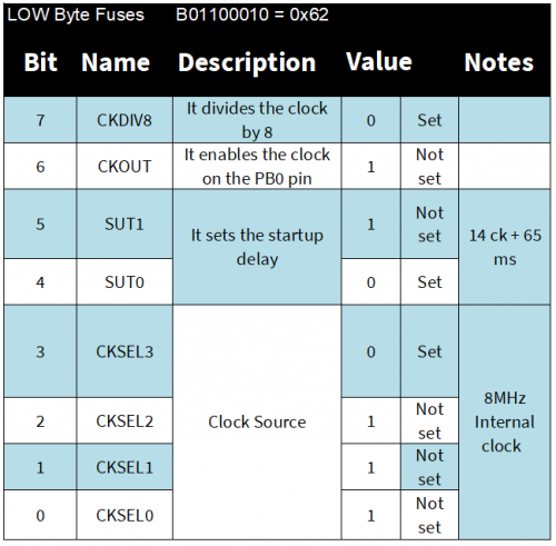
Table 7

Let’s write the Bootloader on the chip
Let’s download the files from the GitHub repository, that may be accessed from https://github.com/LowPowerLab/DualOptiboot by clicking on the green “Clone or Download” button, as shown in Fig. 4.

Fig. 4
Let’s download the DualOptiboot-master.zip zip file, then unpack it into a temporary folder: for example, C:\TMP\. We are interested in the file found in the following path:
C:\TMP\DualOptiboot-master\DualOptiboot_V5.0_atmega328_BlinkD9.hex
The indicated file is the bootloader that is suitable for our ATmega328p microcontroller, it has the notification LED set on the D9 I/O pin.
When on BitBurner, let’s locate the Tab indicated as “AVR Memories” (Fig. 5), and select the bootloader file to be uploaded, then while in the “Memory Programmer” combo box, let’s select “Flash Only” and click on the “Write” button.
At this stage, we should see a progress bar in the Log window: it shows the loading progress and, once the operation is complete, a reassuring message that tells us that the loading reached a successful ending.
If everything goes like this, we are all set: our Antennino now has a beating heart and is ready to host our sketches.

Fig. 5
Conclusions
Well, this second and final instalment about Antennino ends here; we explained what a bootloader is, and all of its peculiarities, in detail; then we moved on to the bootloader and its selection, and to the program with which to upload it into Antennino’s microcontroller, and then to the installation procedure, so that Antennino may be managed from Arduino IDE by means of the computer’s USB connection. Now that you have the bootloader you may install your sketches.
In a future article, we will start to program Antennino, starting from a Hello World sketch that will, however, use two modules: one for the purpose of simulating a sensor node and the other one for the implementation of a simple gateway.
Therefore, please stay “connected” and you will discover new and useful developments of this project.
From openstore
Pololu USB AVR Programmer v2.1
