It supports various low-cost GSM/GPRS modules in order to provide cellular connectivity to our Arduino projects. First part.
Given the growing demand for electronic equipment with connection to the GSM/GPRS network, we decided to develop a new GSM shield for the Arduino and Raspberry Pi 3 platforms, capable of supporting various modules on GSM breakout boards developed by open electronics, which use SimCom, Quectel and Fibocom GSM motors on the same pinout. Then you can try and find the GSM module that best suits your application, develop the firmware on the shield and then integrate the chosen module into the final circuit. The shield allows you to take advantage of both the functions of voice call and SMS exchange and for the management of GPRS data connections. In the latter case, the SIM card must be enabled for data traffic.
Applications that make use of simple SMS can be systems that, given the occurrence of an event, must send a text, with simple related data, to a mobile phone.
The data connection is useful in applications where you need to send or receive data from or to a server.
While a typical application that could benefit from a GPRS connection could be an electrical energy monitoring system that periodically sends to a server the electrical measurements made.
Block diagram
Before analyzing the electrical scheme, let’s dwell on its composition, described by the block diagram proposed in this page. Let’s start with the main power supply, which is taken through a µUSB connector to which you can connect a power supply like that of mobile phones, or you can connect the USB cable directly to a PC USB socket type A, taking the power from it. The 5 volts of the µUSB connector is taken both to the DC/DC converter, to generate the supply voltage of the GSM modules (+VBAT) and to the headers for the Arduino and Raspberry Pi boards.
In the block diagram, the Arduino and Raspberry Pi boards are represented by two green functional blocks, from which some lines of communication, diagnostics and debugging start.
But let’s proceed in order: first of all, we can observe that from the functional block corresponding to Arduino there are several UART communication lines, both hardware and software assigned; the latter are I/Os that can act as serial libraries and are useful, for example on Arduino Uno R3, where there is only one hardware UART. If this is to be used to debug the firmware through the serial monitor, if you want to communicate with the GSM module you must initialize a virtual serial. Is anyone wondering why we’ve set up two UARTs? The choice comes from the fact that there can be GSM modules equipped with two UARTs: for example the SimCom SIM928A, which integrates a GPS receiver and has a serial port to receive AT commands for managing the GSM/GPRS section and the other for reading the NMEA GPS data regarding the positioning.
As for Raspberry Pi, it only provides one hardware UART; in this case, it is not possible to have two simultaneous communications.

The UART lines, in the case of Arduino boards, before reaching the GSM modules pass through level shifters that allow to couple data lines with working voltages at +5V with data lines with working voltages at +3.3V. This is not necessary with regard to Raspberry Pi boards, as these already work at +3.3V voltage. In addition to the level shifters, the UART lines before reaching the GSM modules meet a series of 3-position jumpers useful to select whether to use a communications hardware rather than software and decide if you want to enable/disable the communication light to see what commands are exchanging the Arduino/Raspberry Pi boards with GSM engines. It is also possible to route the signals in order to send the AT commands directly from the PC, this is very useful during the study phase of the commands to verify their correct operation before code them in the Arduino and Raspberry Pi boards. These level shifting and signal routing sections are represented by grey blocks (they are in all three distinct blocks, two named “Level shifter and jumper selector” while the third is only a “Jumper selector“).
The GSM engines section is represented by the yellow block “GSM BreakOut Board” to which the previously discussed communication lines arrive. In addition to the data lines, this block also includes the +VBAT power supply generated by the DC/DC converter and the Vrtc power supply made available by the 0.22F gold foil capacitor used to keep the Real Time Clock Calendar on the GSM modules powered in the event of a primary power failure. The charge of the capacitor is guaranteed by the same electronics of the GSM modules when it fails the capacitor will keep the RTCC active until it is completely discharged.
The GSM modules are also connected to two buttons which are used to turn on/off the GSM motor, button P1, or to reset the GSM motor, button P2. These buttons are useful when you have to operate the motors manually, for example, switching them on and then sending AT commands from a PC. The duration of the on/off pulse, rather than the duration of the reset pulse, depends on the motor itself. Therefore, it is necessary to consult the datasheets for more details, of course, we are talking about pulses of very short duration. We conclude the roundup with the MIC and SPK lines, differential lines, which are used to connect respectively a microphone and a speaker, useful during voice calls.
Now let’s examine the orange block “GSM/GPRS SPY” which, as mentioned before, is used to spy on serial communication between GSM engines and Arduino/Raspberry Pi boards, rather than sending AT commands directly from a PC. The function block is very simple and includes logic ports and a few jumpers for signal routing as well as a 4-pin connector, blue block adjacent, to which connect the USB/UART converter FT782M, sold on the open electronics store.
We conclude the analysis of the block diagram by saying that the Arduino/Raspberry Pi boards are connected to two P3 and P4 buttons for future developments and a series of digital lines for debugging the firmware that you will write. In particular, we have three lines of triggers, with related LEDs, plus six diagnostic LEDs: two red, two green and as many yellow; they are useful during the phases of GSM engines initialization, sending and receiving SMS, voice calls, etc.
With this, we have concluded the analysis of the block diagram. We can then move on to the detailed description of the wiring diagram.
Wiring diagram
Let’s start with the power supply section, which draws voltage through the micro USB connector, from which the 5V reach the integrated U2 which is a step-down voltage regulator. In detail, we used an LM2596, D²PACK package, with output voltage adjustable from a minimum of +1.23V to a maximum of +37V.
For our application, we have set the output voltage to +4.1V because the GSM modules expect a stabilized power supply between +3.2V and +4.8V. The integrated LM2596 guarantees an output current up to 3A with a standby current of 80µA, accepts input voltages of up to +40V and the working frequency of the switching section is 150kHz. Fig. 1 shows the block diagram of the voltage regulator highlighting the operating logic and the various input/output and control pins. As you can see, at pin 1 the input voltage is brought while from pin 2 the output switching voltage is taken, which through the network formed by the Schottky diode, the inductance and the low ESR capacitor returns the regulated output voltage to the desired value. The voltage value is obtained by feedback with resistive divider to be connected to pin 4 of feedback.

Fig. 1
A digital input, pin 5, is available to turn the voltage regulator on/off. The logic is active low and in our application, we force it to ground or always on. The operating principle of the voltage regulator can be summarised in the diagram in Fig. 2.
The integrated works on two distinct periods of time, the first period is given by the ON switch condition and the second by the OFF switch condition. In the ON switch condition, the input voltage is connected directly to the inductance input and the recirculation diode is prohibited. During the OFF period, the switch is open and the voltage on the inductance reverses its polarity and triggers the recirculation diode. The current flows through the diode keeping the current loop with the load. The frequency at which the electronic switch is switched on/off is 150kHz as indicated above.
The converter control is obtained by varying the duty-cycle or by acting on the ON and OFF times of the switch as indicated by the following:

Having said that, let’s calculate the values that the feedback resistors must take to set the output voltage to the regulator. The formula to be followed is the following (with reference to Fig. 1):

which when applied to our circuit becomes:

The power supply is then brought to the GSM modules, i.e. the connectors marked as U5 and U6, and to the P1 and P2 buttons, respectively used to manually switch the modules on/off and reset them (manually). The LED LD1 indicates the presence of the +VBAT power supply. Instead LD2 is used to indicate the presence of the +5V power supply and finally, LD3 indicates the presence of the +3.3V power supply returned by the Arduino boards, rather than Raspberry Pi.
The +5V supply voltage is also transferred via a voltage divider to the X1 terminal block, o that a voltage reference is available for external electronics for future development. The X2 terminal block and the P channel MOSFET Q4, used as an electronic switch, complete the set-up.
If the MOSFET Q4 is switched off, i.e. the VGS voltage does not exceed the channel activation threshold, the +5V supply voltage, through the internal diode of the MOSFET, reaches pin 1 of the X2 terminal board. Now, if the signal “shutdw” is set high, it happens that Q3 is switched on by grounding the gate of Q4 and, thanks to the voltage present on pin 1 of X2, the VGS exceeds the threshold by activating the Q4 channel. In this condition, when the main power supply fails (+5V) and if there is a +5V voltage generated by an auxiliary board on the terminal block, our electronics will continue to operate until the “shutdw” line is turned down.
Let’s now describe the interconnections present on both the Arduino and Raspberry Pi boards. Supported Arduino boards are Arduino Uno R3, Arduino Mega 2560 R3 and Fishino boards (Uno and Mega). In case you use Fishino boards (use boards with the implemented latest firmware that frees I/O 7) you must remember that I/O 10, 11, 12 and 13 are used for WiFi and in case you use the microSD card also I/O 4 must be free. Since at I/O 10, 11, 12 and 13 we had planned to connect the P4 button and three triggers for debugging, this should be taken into account when using the Fishino Uno board. If you use the Fishino Mega board, the I/Os to be left free are 4, 10, 50, 51 and 52 (also in this case use boards with the implemented latest firmware that frees I/O 7). If I/O 11, 12 and 13 are to be free, move jumper J12 to position 2-3.
As for the Raspberry Pi boards are supported: Raspberry Pi 2 model B+, Raspberry Pi 3 model B and Raspberry Pi 3 model B+.

Fig. 2
Let’s start with the Arduino boards, for convenience, we used as a starting reference the Arduino Mega board pin-out with the corresponding pins of the Arduino Uno board highlighted in blue. If you use the Arduino Mega board, you can choose whether to use the two hardware UARTs, UART1 and UART2, mapped to I/O pins 16, 17, 18 and 19 or the two software UARTs that are mapped to I/O pins A8 (RX UART2), A9 (RX UART1), A10 (TX UART2) and A11 (TX UART1). The corresponding I/Os for the Arduino Uno board are A0, A1 A2, and A3. The software UARTs, as far as the reception signal is concerned, must be mapped on the I/O pins that support the port change interrupt. So be careful when developing any hardware for your applications.
The TX and RX signals of the two UARTs, both hardware and software, must undergo a level adjustment as the Arduino boards work with logical levels at +5V while the GSM modules work with the level at +3.3V. Then the TX signal, before reaching the GSM engine, is adapted through the use of a MOSFET channel N properly connected. The same goes for the RX signal from the GSM module to the Arduino board. To better understand what has been said, let’s examine the connection of the TX and RX lines, both hardware and software, used to send AT commands for the management of the GSM section. As can be seen from the wiring diagram on the Arduino side, the affected lines are identified as “ARD_RXD1_HW”, “ARD_TXD1_HW”, “ARD_RXD1_SW” and “ARD_TXD1_SW”.
These come to selection jumpers, J6 and J7, which are necessary to decide whether to use a hardware or software serial connection. Therefore, if the jumpers are in position 1-2, a software UART connection is identified, while if the jumpers are in position 2-3, a hardware UART connection is identified.
As for the Arduino TX signal, whether hardware or software, it reaches the MOSFET Q5, which adapts the voltage level to +3.3V comparable with the electronics of the GSM modules. In addition to the MOSFET Q5, two unassembled resistors in voltage divider configuration have been prepared to adapt the voltage level from +5V to +3.3V (Only for the TX line). As for the RX signal, always on the Arduino side, we have that this is brought to the drain of the MOSFET Q1 that so connected allows you to adapt the signal from the GSM motor at +3.3V to the voltage level +5V of Arduino. We have already used this type of adaptation in many other applications.
The same reasoning has been applied to the TX and RX lines for the management of the AT commands of the GPS and therefore referenced to the J8 and J9 jumpers.
As mentioned, it is possible to spy on the AT commands that are sent to the GSM/GPS module and the relative answers using the electronics formed by the integrated U1 and the jumpers J1, J2, J3, J4 and J5.
To complete the light, we have the usual USB/Serial converter FT782M configured to work with I/O at +3.3V logic level and inserted in the appropriate connector CN1. Thanks to this electronic piece and to a proper configuration of the jumpers it is possible to do the following:
1) spy on AT commands sent to GSM/GPS module from Arduino/Raspberry Pi board;
2) spy on the AT commands sent to the Arduino/Raspberry Pi board;
3) send AT commands directly from PC excluding Arduino/Raspberry Pi TX and RX lines.
So, if you want to spy on AT commands, and their answers, sent to GSM module jumpers J1, J2, J3, J4 and J5 must be in position 1-2. If you want to spy on the data received from the GPS modules, jumpers J1, J2 and J3 must be in position 2-3 while jumpers J4 and J5 must be in position 1-2. If you want to send AT commands directly from a PC, for example, to study new commands to be implemented in Arduino or Raspberry Pi sketches, you must configure the jumpers as follows: jumpers J2 and J3 in position 1-2, jumpers J4 and J5 in position 2-3 and jumpers J1 indifferent (configuration for sending AT commands to GSM section). Or jumper J2, J3, J4 and J5 in position 2-3 and J1 indifferent (configuration for reading GPS data).
To exclude the possibility of sending AT commands from the PC permanently, simply do not mount the two 0 ohm resistors R2 and R3. In this way, it is impossible to send AT commands from the PC to the GSM/GPS engine because the line is interrupted.
However, we recommend that you always mount the spy section, as it is useful during the study and learning phases of the AT commands.
Moreover, given the possibility of using a PC terminal to send/receive AT commands, there is a fast and effective method of study that frees you from any bugs introduced during the writing of C code for the development or integration of an Arduino/Raspberry Pi library. In other words, first, you study the AT command you want to implement using a PC terminal and then, only after understanding how it works, you implement it in your library.
Returning to the TX and RX communication lines, those coming from Raspberry Pi already have levels compatible with GSM modules and therefore do not require line adaptation. However, it is necessary to decide via jumpers J10 and J11 whether to drive the GSM section rather than the GPS section. If J10 and J11 in position 1-2 will communicate with GSM section, vice versa if in position 2-3 will communicate with GPS section.
In addition to the TX and RX lines, we have also prepared the control lines which, however, are currently not used in our library, namely the lines “CTS“, “DCD“, “RTS” and “DTR“.
Much more important are the “ON/OFF” and “RST” lines, which are used respectively to switch the GSM/GPS module on/off or to reset it. Fig. 3 shows how the electronics needed to switch the GSM module on/off must be set up, as you can see the ignition pulse must be positive logic and its duration must be longer than one second.

Fig. 3
Fig. 4 shows the time diagram for switching on the GSM module and, more precisely, shows the trend that the PWRKEY signal on the transistor collector must have. Therefore, in order for the GSM ignition operation to be successful, it is necessary that, after having given power, you wait at least 500ms before sending the ignition pulse (which must last more than 1 second).

Fig. 4
In addition to switching on the GSM using the appropriate line, we have prepared the button P1 that performs the same task, providing the logical level 1 because it must activate the transistor that sets the PWRKEY module to zero internally.
Fig. 5 shows the trend that the PWRKEY signal must have when the GSM module is switched off: the logic zero pulse must have a duration of more than one second but less than 33 seconds. The time diagrams just shown referred to a SIM800C engine. If other motors are used, such as an M95 from Quectel, the duration of the on/off pulses may be different. In this case, the shutdown pulse must have a duration of between 700ms and a maximum of one second. Therefore it is always good practice to consult the module datasheet.

Fig. 5
In addition to the on/offline, we have set up a reset line (“RST“) which serves to reset the GSM motor. Push-button P2 performs the manual reset function.
We conclude this review with the “RI” line, called “Ring Indicator“, which is brought to the input INT0 (Arduino Uno) or INT4 if it is ArduinoMega. This line, active at a low logic level, indicates the reception of an SMS or a voice call. If we take as reference a SIM800C engine we have that during the reception of an SMS the line goes low for 120ms and then returns high. On the other hand, if you receive a voice call, the line goes low and only returns high if you answer or reject the voice call with the appropriate AT command.
Fig. 6 describes the signal trend on the RI line (Ring Indicator) with regard to the reception of an SMS while Fig. 7 shows the trend during the reception of a voice call.

Fig. 6
Note jumper J13, which can be used to force GSM modules to boot in case the firmware needs to be updated.

Fig. 7
GSM modules usually have an audio section to which you can connect a microphone and speakers to make voice calls, usually use a headset with a microphone equipped with a microphone audio jack separate from the speakers jack, or (most commonly) with a single jack, which however is not standardized but exists in two versions: CTIA and OMTP (Fig. 8a ).
The difference is in the contact of the microphone, which is in different positions. Our electronics are designed to work with both OMTP and CTIA formats: by mounting resistors R54 and R55, the CTIA standard is selected, while by mounting resistors R52 and R53, the OMTP standard is selected. The connector used SJ-43514, JK1, is a 3.5mm jack of the CUI-INC which has the pin-out shown in Fig. 8b, where you notice the correspondence between the jack in OMTP/CTIA format and the contacts of the connector, as already widely said, the only difference between the two formats is that the microphone line and the GND are inverted.
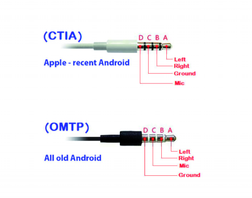
Fig. 8a
The audio section is completed by a series of capacitors to be connected on the differential lines of the speakers and on the differential lines of the microphone. As for the speaker capacitors, there are two blocks; one to be connected near the GSM and the other near the connector. The SPK_P signal is carried by the C37 and C38 capacitor to the two audio connector speakers left and right.
All we have to do is describe the trigger and debug lines, which are useful for code development at both the library and sketch level. On the Arduino board, the “Trigger1, 2 and 3” trigger lines have been prepared and carried by means of series resistance to the CN3 connector to which an oscilloscope probe can be connected, depending on the case. Trigger lines are based on I/O pins 11, 12 and 13. Remember that in the case of Fishino boards these pins are shared with the WiFi section. They complete a series of LEDs connected to I/O 32, 33, 34, 35, 36 and 37 and available only on Arduino Mega and Fishino Mega boards. Both the trigger lines and the LED lines have been brought to the Raspberry Pi board.

Fig. 8b
PCB Layout
Let’s have a brief look at the board layout, proposed in Fig. 9 that shows the sections each one distinguished by colour:
- orange section, where you can find the power supply carried by the micro USB connector, the terminal block for connecting a possible battery backup system, the audio jack and two auxiliary buttons for future developments;
- green section, where the jumpers for the selection of the various communication modes and indicator are located (you will find a summary table below);
- grey section, where there are two connectors for housing the GSM breakout boards;
- red section, where there are the trigger and diagnostic LEDs as well as the comb connector for the connection of a possible oscilloscope probe;
- blue section, where the two buttons used to turn on/off the GSM engine and the reset button are located.

Fig. 9
The shield is available in a pre-assembled version, but for those who want to try to mount the components on the board, we suggest to start from the integrated U11 followed by Q1 and U2. Then you have to mount all the resistors and SMD capacitors in 0603 cases, the two connectors U5 and U6 and then the remaining SMD components starting from the LEDs. Finally, mount the audio jack, the terminal block and all the jumpers and buttons. Leave the interconnect connectors on the Arduino and Raspberry Pi boards for last.
Table 1 summarizes the jumpers and how they should be set.

AT commands from PC via serial light
Many of the AT commands available, in addition to the syntax and the number of parameters associated with them, have more or less articulated responses, consisting of several parameters, which need the code to be decoded and made available to the end user for implementation in your application. Hence, it is essential to be able to study the behavior of the AT commands you want to use before implementing them in your applications or libraries. It is also good to know that in order to achieve certain goals, such as managing GPRS connections, it is necessary to give several AT commands to activate the data connection. We add that in addition to the syntax it is also necessary to study and understand the right sequence of AT commands to be sent because some commands to be received and accepted require the prior sending of other AT commands before them, and they must be sent in the right sequence.
An example of this is when trying to connect to an APN using the AT+CSTT command in a TCP/UDP data connection. Before sending the AT command to connect to the APN you must first send the AT+CIPRXGET command (Get Data From Network Manually) if you do not want to see the error code “3” return, i.e. operation not allowed, by sending the AT+CIPSTART command.
A useful tool for this purpose is the use of software for the analysis and simulation of serial communication protocols. Here are some examples in which we will show some spy sections of the AT commands exchanged between the Arduino boards and the GSM module and the sending of the AT commands from the PC for the configuration of the GSM module to work in GPRS mode.
Fig. 10 shows the serial monitor of the Arduino IDE during the initialization phases of the GSM module: in this case it is a SIMCOM SIM800C.

Fig. 10
When the serial monitor is started, Arduino is reset and the procedure of initialization of the GSM modules is started, including ignition; however, since the GSM module was already switched on, the impulse sent to the engine actually switches it off and this is deduced from the reception of the string “NORMAL POWER DOWN” (see section circled in blue). The initialization algorithm is able to understand these situations and automatically turns on the GSM module again, this is understood by the reception of the string “RDY” (see section circled in red). Then follows a series of AT commands to initialize the GSM engine including sending the PIN code. The information you see in the serial monitor of the IDE can be enabled/disabled via code, this information is very useful during the debugging of the code. However, in order to have a real view of the information exchanged between the engine and the Arduino/Raspberry Pi boards, it is necessary to use a serial light in hardware assisted by special analysis software.
Fig. 11 shows, circled in blue, that the GSM module has been turned off by the library and then on again (in red). Circled in green you can see the AT commands sent to check if it is necessary to send the PIN code to activate the SIM, how many attempts we have available to send the PIN code and the successful activation of the SIM after sending the code itself.

Fig. 11
Fig. 12 instead shows the sending of AT commands from PC to configure the GSM module in GPRS mode, in particular during a data connection to a server via TCP protocol; see highlighted in blue the command “AT+CGATT=1” used to connect to the GPRS service, in green the command “AT+CSTT=”ibox.tim.it” used to connect to your APN (GPRS Access Point Name), in red the “AT+CIFSR” command that returns the IP address assigned by GPRS, in yellow the “AT+CIPSTART” command for connecting, via TCP or UDP protocol, to a remote server and its port. Below is a series of commands for sending data, in particular using the PHP code on the server. The above shows the effectiveness in sending AT commands from a PC to study the steps to be followed to correctly configure a data connection to a remote server. Once you have found the right AT command stream, you can implement it in code in your library and its sketch.

Fig. 12
Updating GSM modules
With the direct connection to the PC, it is possible to update the firmware of the GSM modules; as an example, we will see how to update the firmware of the SimCom SIM800C. First, you need to download the tool, which you can download from the following link:
www.dropbox.com/s/kn73rhcz8v72jhb/SIM800_Series_download_Tools_Customer_v1.06.rar?dl=0.
It is not necessary to install the software because to use it is sufficient to run, in administrator mode, the file “SIM800_Series_download_Tools_Customer.exe” which will open the work window in Fig. 13, where we can select a number of parameters including the Target (in our case, SIM800C), the communication interface (PortType2, which in this case is a UART), the “Com” to which you are connected and finally the Baudrate. The Com used in the example is COM15 and the baud rate set is 115,200.
The next step is to load the firmware, which in the case of SimCom is a file with the extension . cfg. The update should be done with the shield only, because it is essential that the GSM is off. Click on “Start Download” and only then turn on the GSM engine by holding down the power button P1 for more than 4 seconds or, if you prefer, by inserting jumper J14 in position 1-2 until the update procedure starts. The firmware update takes place in three steps.

Fig. 13
Gsm library for Arduino boards
The library architecture is based on a series of C++ files and related .h files with definitions of variables, constants, data structure, etc. The main file, which also contains the procedure for switching on and initializing the GSM module, acts as the basis for the other files that make up the library (Fig. 14).
There are several boundary files to the main one, including:
- UART connection management “cpp“.
- I/O management “cpp“
- management of the interrupts used by the “cpp” library
- SMS management “cpp“
- voice calls management ” cpp “
- security function management “cpp“
- phonebook management “cpp“
- GPRS connection management “cpp”
- HTPP commands management “cpp“.
The files contain the code for managing a series of AT commands both for sending commands, with the relative parameters, and for decoding the responses received by the GSM, including the error codes. Currently, only a few AT commands are managed, but as the library is in continuous development more and more commands will be added in the future. The same applies to the error codes management.

Fig. 14
Fig. 15 shows the state machine for sending AT commands and GSM response management: it starts with the initialization of the GSM engine and then enters a loop for sending AT commands. For each AT command sent, a response from the GSM engine is expected and its content is decoded. If the answer is OK, the next AT command will be passed, otherwise the system will return the error code and, depending on the case, will try to send the AT command again up to a maximum of three times. If the AT command is not successful, even after three attempts, the system resets the GSM engine and starts again by re-initializing the same and then returns to the AT command sending loop.
This is the broad approach that lies at the heart of our library. AT management functions commands that are not used do not take up Flash memory space, however for each category of AT commands there is its own response management section, which is managed by a suitable state-controlled machine. In this case, if enabled with the appropriate #Define, the response management routines are inserted in the compilation of the machine code and then take up space in Flash. It’s all about finding the right balance between the functions you need for your applications and the memory space your library takes up.

Fig. 15
The library supports the Arduino Uno and Fishino Uno, Arduino Mega 2560 or Fishino Mega 2560 boards. In the future, we do not rule out extending compatibility to the most advanced Arduino, i.e. those with a 32-bit microcontroller. Having said that, we shall conclude this first episode here.
List of components
R1: 100 kohm 1% (0603)
R2, R3: 0 ohms (0603)
R4, R6, R10: 1.2 kohm 1% (0603)
R5: 5.6 kohm 1% (0603)
R7: 2,2 kohm 1% (0603)
R8: 200 ohms 1% (0603)
R9: 10 kohm 1% (0603)
R11, R12: 220 ohms 1% (0603)
R13: 1,2 kohm 1% (0603)
R14, R15: 220 ohms 1% (0603)
R16, R18: 5.6 kohm 1% (0603)
R17, R19: 10 kohm 1% (0603)
R20: 1.2 kohm 1% (0603)
R21, R22: 10 kohm 1% (0603)
R23: 220 ohm 1% (0603)
R24. R25: 0 ohm (0603)
R26÷R28: 220 ohm 1% (0603)
R29, R30: 10 kohm 1% (0603)
R31: 1,2 kohm 1% (0603)
R32, R33: –
R34, R35: 10 kohm 1% (0603)
R36, R37: –
R38÷R40: 1.2 kohm 1% (0603)
R39, R40: 1.2 kohm 1% (0603)
R41, R45: 10 kohm 1% (0603)
R42: 36 kohm 1% (0603)
R43: 220 ohm 1% (0603)
R44: 5,6 kohm 1% (0603)
R46, R48÷R50: 1.2 kohm 1% (0603)
R47: 22 kohm 1% (0603)
R51: 10 kohm 1% (0603)
R52, R53, R59: –
R54, R55: 0 ohms (0603)
R56÷R58: 10 kohm 1% (0603)
R60: 0 ohm (0603)
R61÷R64: 10 kohm 1% (0603)
C1: 100 nF 16 VL ceramic (0603)
C2: 10 µF 16 VL ceramic (0603)
C3: 10 nF 16 VL ceramic (0603)
C4, C5: 220 µF 16 VL tantalum (E)
C6, C7: 100 nF 16 VL ceramic (0603)
C8, C9: 10 µF 16 VL ceramic (0603)
C10, C11: 33 pF 16 VL ceramic (0603)
C12, C13, C15: 10 pF 16 VL ceramic (0603)
C14: 33 pF 16 VL ceramic (0603)
C16÷C19: 10 µF 16 VL ceramic (0603)
C20, C21: 10 pF 16 VL ceramic (0603)
C22÷C23: 33 pF 16 VL ceramic (0603)
C24: 10 pF 16 VL ceramic (0603)
C25: 33 pF 16 VL ceramic (0603)
C26, C27: 100 nF 16 VL ceramic (0603)
C28, C29: 220 µF 16 VL tantalum (E)
C30: 0,22 F 5 VL electrolytic
C31, C32: 33 pF 16 VL ceramic (0603)
C32: 33 pF 16 VL ceramic (0603)
C33, C34: 10 pF 16 VL ceramic (0603)
C35: 33 pF 16 VL ceramic (0603)
C36: 10 pF 16 VL ceramic (0603)
C37, C38: 10 µF 16 VL ceramic (0603)
LD1, LD6, LD7: Yellow LED (0603)
LD2, LD4, LD5: Red LED (0603)
LD3, LD8, LD9: Green LED (0603)
LD10÷LD12: Red LED (0603)
P1÷P4: Microswitch
D1: MMSD4148T1G
D2: B340A-13-F
Q1, Q2: BSS123
Q3: BC817
Q4: SPD50P03LG
Q5, Q6: BSS123
U1: SN74LVC2G00
U2: LM2596DSADJG
U3: Arduino Mega 2560 rev.3
U4: Raspberry Pi 3 B+
U5: GSM/GPS module SIM928
U6: GSM module G510/M95/SIM900
L1: VLS6045EX-150M
Miscellaneous:
– Micro-USB B connector
– Jack socket 3.5mm from CS
– 3-ways Male strip (13 pcs.)
– 4-ways Male strip (2 pcs.)
– Jumper (13 pcs.)
– 2×10 poles connector pitch 2 mm female (2 pcs.)
– Strip M/F Arduino 8 ways (5 pcs.)
– Strip M/F Arduino 10 ways
– Strip M/F Arduino 2×18 ways
– Strip M/F Raspberry Pi 2×20 ways
– 4-way Female strip
– 4-way clamp
– Printed circuit S1416 (110x158mm)
From openstore
GSM compact interface with M95
Small Breakout for SIM928 GSM&GPS Module
