Based on Time of Flight technology, the module provides information to a microcontroller regarding distance detected in front of its optical sensor based on time-of-flight of a light impulse.
Contactless distance measurement, therefore employing electronics instruments, is a problem to which technology has been provided various solutions over the years; from a solution based on infrared light to ultrasound measurements to the traditional RADAR working with radio microwaves. In any case, detection takes advantage of measurement of the so-called “time-of-flight” or ToF, which is the time it takes an impulse to reach the object to detect and go back. Existing solutions are selected based on distance to measure, the element which distance is to be determined and environmental working conditions, therefore, in general terms, they are determined based on the application.
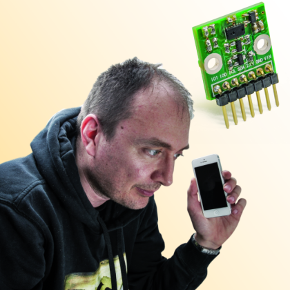
In this article, we want to propose a measurement device, which can be interfaced with a microcontroller and an Arduino in order to take advantage of the ST Flight Sense (ToF) technology to detect symmetry based on the VL6180XV0NR/1 IC; the board allows measurement up to 10 cm (therefore fit for robotics, proximity and gesture sensors) with 1 mm precision and there is a dedicated Arduino library for it, in order to test its qualities and experiment with it, taking advantage of the wide availability of hardware and libraries.
Technology
Before taking a look at the project, let’s discuss theory. In order to make a measurement using the ToF technique, we need to send a wave or a sound vibration towards the object or wall to detect and we detect reflection on it; clearly, this only works if the object or wall surface is not going to excessively absorb the energy. Measurement is based, as mentioned earlier, on the time it takes for an impulse to go from an emitter to the surface of the object to detect, and then go back to the sensor; distance (d) is determined as the product of impulse propagation velocity (v) times half of that time (t) according to the relation:
d = v x t/2
Propagation velocity depends on the medium in which the measurement is taken and in our case, we supposed to work with air.
If we use ultrasounds, which propagation velocity is 340 m/s, if an impulse were to return after 100 ms, that would mean the distance between the emitter and the reflecting objects is:
d = 340 m/s x 50 ms = 17 m
if measurement is taken with a light radiation (conventionally set at 300,000 km/s), time intervals are greatly reduced; for instance, a 100 ms interval would be equal to:
d = 300.000 km/s x 50 ms = 15.000 km
In our sensor, since we are going to make very short-distance measurements using light radiation, it is mandatory to use electronic devices with very low latency time in order to prevent their response delay from influencing the measurement. In order to understand this, we have to consider how the measurement is taken: when the emitter is powered on, a counter is triggered which will stop when the receiving device is excited by the reflected and returned to radiation. The measurement is influenced both by the response time of the emitter (time elapsed from the moment power is activated to when radiation originates from the emitting surface) and the receiving sensor (time elapsed from when the photons of the radiation reach the sensible surface to win the corresponding electric signal is registered). Another error is the one due to counter’s latency and the various logic components.
Those times, considering the very short travel intervals of light impulses must be reduced to a minimum. Useful method to limit the error (which is mandatory in order to obtain a high degree of precision, especially on short distances) is to place a second light sensor towards the emitter (but without covering its emitting surface) so that it will detect light the very moment it comes out; in theory this will compensate the response delay both of the emitter and the sensor.
With that said, we can talk a little about ST technology, which is patented and named Flightsense; this kind of devices are enclosed in one SMD module integrating the Photon Avalanche Diode (SPAD) array light sensor, a traditional Ambient Light Sensor (ALS) and a Vertical Cavity Surface-Emitting Laser (VCSEL) operating at 850 nm, so in full infrared spectrum. This technology is ideal in order to make, besides devices to measure proximity and short distances, also gesture detectors. The ambient light sensor has a great sensitivity: less than 1 Lux at 100.000 Lux.
An innovative feature of this technique is that it allows making measurements which are basically independent of the light reflection constant of the surface to measure, thanks to a special circuit that allows to regulate the gain of the light receiving stage and environment light and to emit very short impulses.
What’s peculiar about this module is that on the light sensors side it incorporates a second light detector that is used to determine ambient light, in order to obtain a signal which is subtracted, since it is uniform, from the impulsive one coming from the reflected returning laser; this way, amplitude of the received signal accurately reflects its distance.
In other words, it is easy to discriminate ambient light by knowing when light impulses start and waiting for them to come back, while ambient light is somewhat constant.
The sensor’s presence is fundamental in applications like proximity detectors placed behind the glass of a tablet, smartphone or touch panel, because it allows differentiating reflection of part of the light radiation emitted by the laser diode, on the internal side of the glass, which would trick the photosensor on its way back.
Figure proposes a simulation of how the sensor works, with the IR light emitted by the laser bank and the sensors reception cone in green, with the related aperture angles, as you can see, reception angle of the photosensor is clearly superior to the laser’s emitting angle, which should ideally be zero, since the best solution would be to emit a ray that doesn’t fan out, collimating ad infinitum.
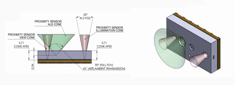
Basically, a conically shaped ray allows locating objects more easily, especially the smallest ones.
Elimination of reflected light is fundamental in this case, not just for the level of disturbance overlap in the return signal, but more importantly for calculating time-of-flight of the light impulse, since the reflected wave inside the glass would arrive before the light reflected by the object which distance is to be measured, thus determining a measurement error with a short measured distance.
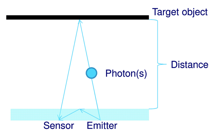
Figure shows a diagram of how the device works: the laser diode (emitter) emits periodic light impulses of which one part is reflected and comes back to the sensors; by synchronizing impulse emission and waiting period (it can be done by supposing a range of time intervals and an emission frequency) we can remove the disturbance caused by the ambient light, thus increasing the device’s sensitivity.
On the other hand, typical IR proximity measurement devices are based on the intensity of the reflected wave, which makes them not so reliable because that depends on the reflective parameter of the surface of the objects to be detected.
The particular thing about the diode used is that it is a Single Photon Avalanche Diode, which is a photodiode that must be inversely polarized as every photodiode (with a load resistor connected in series) which works in the avalanche effective zone, in the third quadrant. Work cycle is described in the figure.

By maintaining an inverted anode-cathode voltage close to breakdown voltage on the diode, when the surface is hit by the light, the first photon triggers conduction due to avalanche effect and current strongly increases, then it drops to zero when voltage goes under the breakdown threshold (Vbd in the diagram). Now another photon is needed to trigger conduction. With an array of SPAD diodes, we can count the photons.
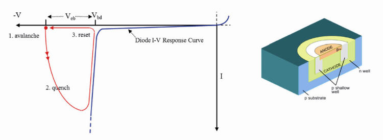
At the ends of the load resistor, we can then register a very short impulse corresponding to each photon, which theoretically allows to detect and count the single photons which are, according to quantum theory, the energy particle composing light radiations.
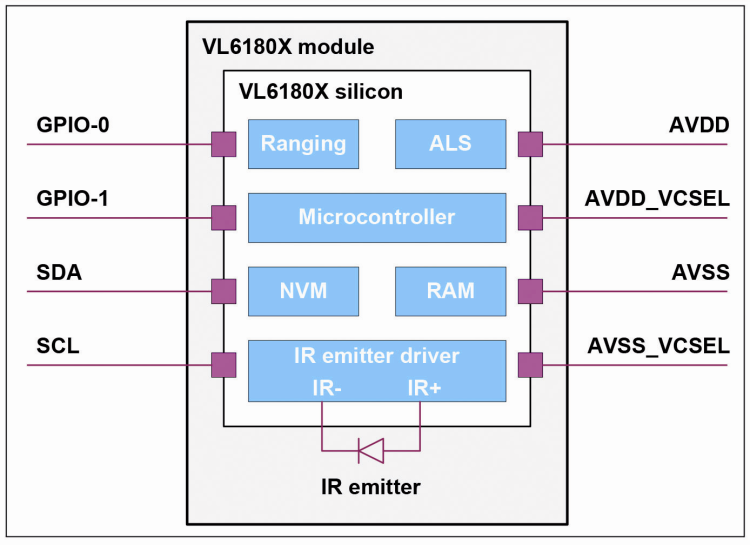
The ST integrated circuit is powered through the AVDD (positive) and GMD (ground) pins for the receiving section and through the AVDD_VCSEL and AVSS-VCSEL pins for the laser diode; it has two GPIOs that are typically used as inputs (on which we can apply pull-up resistors, as shown in the electric diagram of our circuit) to handle some functions. Communication with a host device, which is usually a microcontroller, takes place on the I²C-Bus composed by the SCL (5) and SDA (6) pins, which are respectively clock and bidirectional data channel; by using the bus (working at 400 kHz) we can set functioning mode, sensitivity etc., but also read the measurement result.
In terms of functioning, we have to mention that the device can measure either at set time intervals and on demand (this mode allows to optimize consumption, which is largely due to the laser powering on).
In order to adapt voltage levels of the ST device to the TTLs, a bidirectional shifter has been employed, with the circuit section centered on the two MOSFETs, which functioning can be analyzed line by line and logic level by logic level; we are going to do it shortly when studying the electrical diagram.
Circuit diagram
Now that we have explained how the technology at the base of our device works, it is time to take a look at the circuit application, that we have made as a breakout board in order to better integrate it into various systems.
The circuit diagram includes, besides the VL6180XVONR/1 IC, a linear voltage regulator with low dropout (U2) and a MOSFET adapter for the I²C-Bus interface that is used to shift logic levels 0/2,8 V of the integrated to adapt them to the standard TTLs of traditional logics boards and Arduino’s.
In order to explain how the shifter works, let’s start from the clock, which is connected to the 5-pin line on the U1 side, while it is connected to the SCL on the pin-strip side (both lines are equipped with a pull-up resistor), when the connector’s SCL is at logic level high, the protection diode inside the MOSFET (placed between drain and source) is interdicted because the source is negative (at 2.8 V) compared to the drain (which is capped at 5 V by R5) and even though the impulse doesn’t reach U1’s SCL, the latter is at logic level 1. On the other hand, when the SCL contact of the pin-strip is at logic zero (0 V), the MOSFET is still interdicted (because it’s gate is polarized at two about 8 V) but its protection diode is in conduction, since the source is at 2.8 V why the cathode is at the zero, therefore level low on the SCL drags the 5-pin of U1 to logic zero (0.6 to be exact). SCL channel is unidirectional, therefore there is no opposite situation, i.e. U1 gets the clock from the host.
Let’s talk about the SDA now, by analyzing the case when the host sends out the data: when SDA is at logic zero, the protection diode of Q2 is in conduction and drags the source to 0,6 V and 6-pin of U1 along with it; instead, when it’s at 5 V, both MOSFET and diode are interdicted, therefore U1’s SDA goes to 2.8 V (level high) thanks to the pull-up resistor R7. If it’s VL6180 the transmitter instead, when it puts its 6-pin to logic zero, the Q2 MOSFET conducts electricity between drain and source, because its source is at 0 V while the gate is at 2.8 V, therefore its drain current drags to around 0 V the connector’s SDA, due to voltage drop on R6 pull-up resistor; on the other hand, when 6-pin of U1 is at logic level high (2,8 V) source and gate are at the same voltage and the MOSFET stays in interdiction, leaving the R6 pull-up resistor to keep SDA line to logic 1 (at 5 V) leading to the pin-strip.
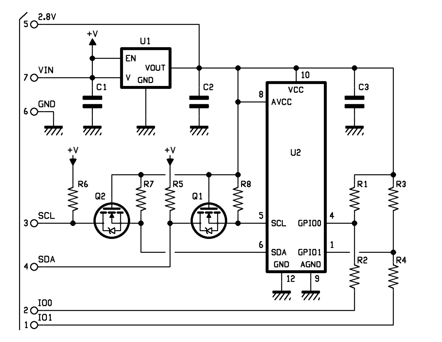
As for the voltage regulator, it is a MIC5219 by Micrel and it is a LDO – available in various versions with output voltages ranging from 2.5 V to 5 V – capable of a current of 500 mA, contained in a SOT-23-5 enclosure with a voltage of just 0.5 V between IN and OUT pins; it is very temperature-stable and it includes a short circuit protection at a high-temperature protection on the output, besides a protection from polarity inversion at the input.
The integrated circuit can be shut down (in this case it won’t absorb more than a few fractions of micro amps, although powered on) through the EN-pin (logic 1 activates and 0 puts in shutdown), which accepts TTL impulses up to 5 V.
The other pin, the BYP pin, is used to connect a capacitor with ground for better filtering the reference voltage of the error amplifier and therefore minimizing the noise overlapped to voltage coming from the integrated circuit. The capacitor must be picked between 470 pF to 1 nF, although you can also leave that pin disconnected.
Before concluding the description of the circuit diagram, let’s take a quick look at the GPIOs of VL6180XVONR/1 that, as already mentioned, can be configured through dedicated commands on the I²C-Bus; the settings for our project are included in the dedicated library.
Listing1
//Recommended settings from datasheet
//http://www.st.com/st-web-ui/static/active/en/resource/technical/document/application_note/DM00122600.pdf
//Enable Interrupts on Conversion Complete (any source)
VL6180x_setRegister(VL6180X_SYSTEM_INTERRUPT_CONFIG_GPIO, (4 << 3)|(4) ); // Set GPIO1 high when sample complete
VL6180x_setRegister(VL6180X_SYSTEM_MODE_GPIO1, 0x10); // Set GPIO1 high when sample complete
VL6180x_setRegister(VL6180X_READOUT_AVERAGING_SAMPLE_PERIOD, 0x30); //Set Avg sample period
VL6180x_setRegister(VL6180X_SYSALS_ANALOGUE_GAIN, 0x46); // Set the ALS gain
VL6180x_setRegister(VL6180X_SYSRANGE_VHV_REPEAT_RATE, 0xFF); // Set auto calibration period (Max = 255)/(OFF = 0)
VL6180x_setRegister(VL6180X_SYSALS_INTEGRATION_PERIOD, 0x63); // Set ALS integration time to 100ms
VL6180x_setRegister(VL6180X_SYSRANGE_VHV_RECALIBRATE, 0x01); // perform a single temperature calibration
//Optional settings from datasheet
//http://www.st.com/st-web-ui/static/active/en/resource/technical/document/application_note/DM00122600.pdf
VL6180x_setRegister(VL6180X_SYSRANGE_INTERMEASUREMENT_PERIOD, 0x09); // Set default ranging inter-measurement period to 100ms
VL6180x_setRegister(VL6180X_SYSALS_INTERMEASUREMENT_PERIOD, 0x0A); // Set default ALS inter-measurement period to 100ms
VL6180x_setRegister(VL6180X_SYSTEM_INTERRUPT_CONFIG_GPIO, 0x24); // Configures interrupt on ‘New Sample Ready threshold event’
//Additional settings defaults from community
VL6180x_setRegister(VL6180X_SYSRANGE_MAX_CONVERGENCE_TIME, 0x32);
VL6180x_setRegister(VL6180X_SYSRANGE_RANGE_CHECK_ENABLES, 0x10 | 0x01);
VL6180x_setRegister16bit(VL6180X_SYSRANGE_EARLY_CONVERGENCE_ESTIMATE, 0x7B );
VL6180x_setRegister16bit(VL6180X_SYSALS_INTEGRATION_PERIOD, 0x64);
VL6180x_setRegister(VL6180X_READOUT_AVERAGING_SAMPLE_PERIOD,0x30);
VL6180x_setRegister(VL6180X_SYSALS_ANALOGUE_GAIN,0x40);
VL6180x_setRegister(VL6180X_FIRMWARE_RESULT_SCALER,0x01);
}
From that, we can see that GPIO0 and GPIO1 carry out the following functions:
- GPIO0: changes state when acquisition is over and can be used to communicate to the host microcontroller that it can read the measurement;
- GPIO1, if brought to GND, sends the ST device in standby; then, U1 can be reactivated by sending the required configuration for the measurement through the I²C-Bus (so, bringing GPIO back to level high is not enough).
Management library for the VL6180XVONR/1 is from SparkFun and can also be downloaded from https://github.com/sparkfun/SparkFun_ToF_Range_Finder-VL6180_Arduino_Library. In order to use the library, after download you have to copy the folder inside the zip file in the directory “libraries” where Arduino environment is installed.
Arduino demo
Now, we’re going to show you how we tried out the breakout board in combination with Arduino Uno; the figure shows how to connect the board to the extension connectors. As you can see, we are using four wires only, because we are limiting them to power and I²C-Bus lines, since we just need to take some simple measurements in order to try out the ST device characteristics.

Once loaded into the library inside the “libraries” directory where Arduino environment is installed, you can open the IDE, then from the menu Files>Examples you will find “SparkFun VL6180 Sensor” which is the same example used to manage your sensor, the example sketch (which can be found in List 2) is ready to use, therefore we are not going to edit the sketch in anyway. In it, the I²C-Bus connection is initialized with a 400 kHz clock, in compliance with VL6180XVONR/1 specifications.
Listing2
#include <Wire.h>
#include <SparkFun_VL6180X.h>
#define VL6180X_ADDRESS 0x29
VL6180xIdentification identification;
VL6180x sensor(VL6180X_ADDRESS);
void setup()
{
Serial.begin(115200); //Start Serial at 115200bps
Wire.begin(); //Start I2C library
delay(100); // delay .1s
sensor.getIdentification(&identification); // Retrieve manufacture info
// from device memory
printIdentification(&identification); // Helper function to print all the
// Module information
if(sensor.VL6180xInit() != 0)
{
Serial.println(“FAILED TO INITALIZE”); //Initialize device and check
// for errors
};
sensor.VL6180xDefautSettings(); //Load default settings to get started.
delay(1000); // delay 1s
}
void loop()
{
//Get Ambient Light level and report in LUX
//Input GAIN for light levels,
// GAIN_20 // Actual ALS Gain of 20
// GAIN_10 // Actual ALS Gain of 10.32
// GAIN_5 // Actual ALS Gain of 5.21
// GAIN_2_5 // Actual ALS Gain of 2.60
// GAIN_1_67 // Actual ALS Gain of 1.72
// GAIN_1_25 // Actual ALS Gain of 1.28
// GAIN_1 // Actual ALS Gain of 1.01
// GAIN_40 // Actual ALS Gain of 40
Serial.print(“Ambient Light Level (Lux) = “);
Serial.println( sensor.getAmbientLight(GAIN_1) );
//Get Distance and report in mm
Serial.print(“Distance measured (mm) = “);
Serial.println( sensor.getDistance() );
delay(500);
};
void printIdentification(struct VL6180xIdentification *temp)
{
Serial.print(“Model ID = “);
Serial.println(temp->idModel);
Serial.print(“Model Rev = “);
Serial.print(temp->idModelRevMajor);
Serial.print(“.”);
Serial.println(temp->idModelRevMinor);
Serial.print(“Module Rev = “);
Serial.print(temp->idModuleRevMajor);
Serial.print(“.”);
Serial.println(temp->idModuleRevMinor);
Serial.print(“Manufacture Date = “);
Serial.print((temp->idDate >> 3) & 0x001F);
Serial.print(“/”);
Serial.print((temp->idDate >> 8) & 0x000F);
Serial.print(“/1”);
Serial.print((temp->idDate >> 12) & 0x000F);
Serial.print(“ Phase: “);
Serial.println(temp->idDate & 0x0007);
Serial.print(“Manufacture Time (s)= “);
Serial.println(temp->idTime * 2);
Serial.println();
Serial.println();
}
Now you can load the example sketch on Arduino.
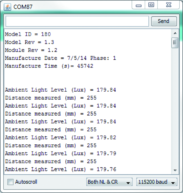
The example sketch initializes the serial connection and then uploads the I²C-Bus to communicate with the breakout board, then it starts a cyclic interrogation of the latter and waits for corresponding data; the same sketch will send the Lux data detected and the object’s distance on the serial port opened for Arduino, therefore in order to visualize this data you have to open the serial Monitor of Arduino with a 115.200 bps baud rate; this way, the monitor window will show such data, as shown in figure, where you can see an example of data provided by the breakout board.
From openstore
TOF (Time Of Flight) module with VL6180 sensor
