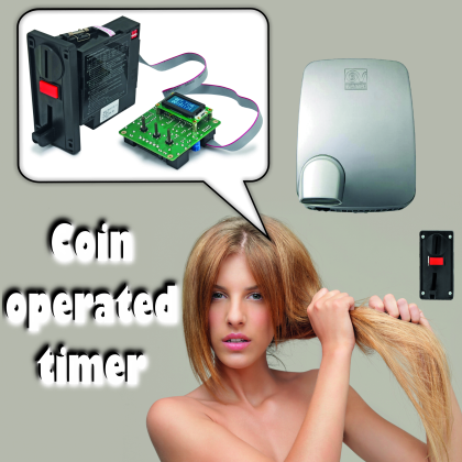
This circuit provides timed access to pay services such as games, showers, blows dryers and various types of vending machines, thanks to a coin counter and a display interface.
In the applications involving the paid access to certain products or services, the electric or electronic “coin-operated actuators” are used, which are devices capable of identifying coins or specific tokens (the older among you will certainly remember tokens for public phones…) and provide an impulse when acquiring the expected amount. Typically, each impulse activates the distribution of a product from a vending machine or the opening of a window or door, but also the faucet of a shower, a hairdryer or a service in a self-service car wash, access to the keyboard of a public computer or a public phone and so on. However, there are situations where, instead of an impulse, we would need a timing feature to start when the coin or the series of corn composing a fare is introduced; this is why we thought of developing the project we are going to describe here. This apparatus recognizes coins from one cent up to 2 euro passing through intermediate measures and provides, on a serial or parallel interface, the information, related to the acquisition of every single piece. In order to convert information provided by the coin-operated device into a specific timing we have created an interface board (Fig. 1) allowing to count pieces and sign to each one a predetermined amount, the timed activation of a dedicated output, in order to obtain a duration of time proportional to the amount inserted, extending the possible applications to many fields and services with various fares.
[bctt tweet=”How to build a Coin-Operated timer with a #PIC18F46K20″ username=”OpenElectronics”]

Fig. 1
To be more specific, through the interface and board we can time the open-collector outputs of the coin-operated device in order to operate, for instance, the shower of a beach resort or AGM, but also a hairdryer, the vacuum cleaner of a car wash; in more general terms, whenever we need to operate something in a timed manner which is proportional to the coin amount.
The interface board
The coin-operated device used has two interfacing modes: serial and parallel; the first one, sends a set number of impulses on a dedicated output line according to the coin inserted, while in the parallel mode (the one used in our project) it takes advantage of a 6-pin interface, with each of the pins representing a group of coins. In this case, the pin corresponding to the recognized coin is earthed whenever a coin belonging to a group is inserted.
The board we have combined with the coin-operated device (you can see to two units connected in Fig. 2) is basically an interface between the user and the device equipped with 3 keys, a 4-way dip switch and a jumper allowing to configure the unit; moreover, the board reads the status of the open-collector outputs of the coin-operated device and acts accordingly on the status of the two onboard relays. The keys, the dip-switch and the display constitute the user interface, while the coin device is the block labelled U4 in the circuit diagram. The circuit is managed by the U5 microcontroller which is a Microchip PIC18F46K20 with 8-bit RISC architecture, 1kB data EEPROM, program flash for 16-bit instructions and computing power up to 16 MIPS, obtained with a 16 MHz clock; the clock is obtained by the internal oscillator (which is very precise and calibrated at 1% in the factory) synchronized by an external quartz or working independently. The oscillator has a PLL and in theory, it can work up to 64 MHz. As with all the latest microcontrollers by Microchip, this can work between 1,8 and 3.6 V, in fact, it is powered by a 3.3 V regulator in the circuit.
The microcontroller, after the power-on reset, initializes its I/Os setting RB0÷RB5 as pull-up inputs for reading the outputs of the coin-operated device and RC7 as output used for handling the INI input, which is the coin collecting restriction input; INI, once activated, prevents the coin-operated device to accept coins even if these are recognized and, in our case, it is used to avoid that once a coin is inserted, it would accept more and take them away from the user. In fact, once a certain timing has been launched the system will no longer consider signals provided by the coin-operated device, therefore the added cash would be ignored.

Lines RC0÷RC6 are initialized as outputs and are used to manage the display on an image visualization level (4 bits plus E and RS criteria) and for what concerns the backlighting (RC6, which lights up the LEDs through the T1 transistor by earthing the BL- line, while the BL+ line is fixed at 5 V). The display we have chosen is a “small” 8 characters display on two lines. Please note that although the display works at 5 V, its outputs also accept 0/3.3 V logic levels provided by the I/O lines of the microcontroller; this keeps us from using voltage translators.
As for lines RB6, RB7, RE3, dedicated to reading keys P1, P2 and P3, we have connected each one to an external pull-up resistor which ends on the positive side of the 3.3 V; those lines are repeated on the CNP connector, which will allow bringing the keys outside, if you like. RA0÷RA3 I/Os are also initialized as inputs, in this case, they are aimed at reading the status of the 4-way dip-switch labelled DS1. These lines of the microcontroller, since they cannot have an internal pull-up, are also equipped each one with an external resistor connected to 3,3V (they are R15, R16, R17 and R18).

Fig. 2
RD0 and RD1 lines are initialized as bidirectional I/O the former and as output the latter and are dedicated to interfacing with the RTC IC, which is U3 via the I²C-Bus; this integrated circuit is a DS1307 and, since it works at 5 V, we had to use a level adapter composed of Q1 and Q2 MOSFETs, which allow to covert the impulses provided by the microcontroller in TTL and those sent by the U3’s SDA in 0/3.3 V. For what concerns the bidirectional line, the functioning of this translator is like this: when SDA is at high level (5 V) thanks to the pull-up resistor R2, the Q1 MOSFET is in interdiction and R1 resistor keeps pin 19 of the microcontroller at 3.3 V, thus determining the logic 1; on the other hand, when the U3’s SDA goes to logic zero, through the protection diode of the MOSFET, the condition passes on the RD0 of the microcontroller even if Q1 stays in interdiction. Now, let’s see how this translator behaves when the micro transmits data towards the RTC: a high logic level on pin 19 keeps the MOSFET and its diode in interdiction, but still determines a logical 1 on the SDA of the U3 because that is done by the R2 pull-up resistor; instead, when the microcontroller transmits the logic zero, the Q1 MOSFET goes into conduction because its source is at 0 V and the gate is polarized by the 3.3 V, so the drain drags the U3’s SDA line to zero.
With that said, let’s talk a bit about how the Real Time Clock DS1307 integrated works, which we wanted in the circuit to keep score of system time and data without giving this task to the Microchip microcontroller; DS1307 is an integrated circuit by Maxim-Dallas containing a low consumption BCD (Binary Coded Decimal), which counts seconds, minutes, hours, days, months and years, provided with 65 bytes of static, non-volatile RAM; the component automatically determines which are the months with less than 31 days and corrects for leap years. The clock can work both following the 12 or 24-hour format, with an indication for a.m. and p.m. hours. Information regarding time and date are saved in a dedicated register and transferred to the outside of the microcontroller (upon request) through the I²C-bus on the chip (SDA and SCL). Besides that, the DS1307 has a programmable clock output that provides a square wave obtained by the clock frequency of the clock (which is in turn determined by the 32,768 kHz quartz connected to pins 1 and 2) which, through a dedicated internal divider, can be reduced to 1 Hz, 4096 kHz, 8192 kHz (it can also provide the whole clock).
The DS1307 also has a control circuit which can check the lack or insufficiency of main power (Vcc) and make so that the voltage needed for its functioning is taken from the backup battery; in our case, it is a 3 V CR2032 button battery (BAT1), guaranteeing an autonomy of around 6 months in case of no power and which is between pin 3 (VBAT) and ground (pin 4, which is GND).
The power control section is sized in order to carry out two tasks: preserving memory in which current time and date are saved and keeping the watch counter ticking. The first task is carried out by preserving the corresponding information in the non-volatile RAM, while the second one is carried out by the backup power taken from the battery connected between pins 3 and 4. The power control section intervenes on other functions of the DS1307 as well, by blocking communication with I²C-bus and production of the possible auxiliary clock signal SQW, in order to minimize power consumption. The protection intervention takes place when the voltage read between the main power pin (8) and ground (4) is 1.25 times lower than the batteries voltage.

Now that we have explained the watch section, let’s take a look at the relay outputs, each one refers to an I/O line of the microcontroller initialized as output and piloting an NPN transistor mounted with common emitter, piloted from its base by a resistive voltage divider (R9-R10 for T2 and R11-R20 for T3) which is used as static switch. When RA7 goes to logic level high, it puts T2 into saturation, which powers through its collector the coil of the RL1 relay; same goes for RE2, which puts T3 into saturation when it goes to logic one, which in turn pilots the activation of the RL2 relay. These two relays allow us to activate the service associated to the amount introduced in the coin-operated devices (RL1) and provide a sound signal or another kind of signal when the allotted time available is almost up (RL2); in particular, RL2 will pulsate at the rhythm of 1s/1s towards the end of the available time slots thus signaling that is almost about to expire, starting from the time you will set. Notice that only contacts C and NO are made available from the switch of each relay (we then use the two relays as simple switches and not as deviated…) and we consider the possibility, for all those loads and applications allowing for it, to power the same from the board by providing the switches with the voltage taken from the input line of the +V power line; the respective feature is enabled by closing bridges JP01 and JP01S.
now, let’s move on to line RA4 of the microcontroller, which is initialized as input and equipped with an external pull-up resistor (R19) that we use to read the status of the JPR Jumper.
Finally, we can see lines RD2, RD3, RD4, RD5 connected to CNOUT connector, which is an interface not handled by the firmware at the moment, available for future developments; the 1 contact of that connector is reserved for powering devices and circuits that may be connected to the board, and it can be set at 5 or 12 V according to how JOUTV Jumper is set.
We end the description of the circuit diagram with the power section, which starts with PWR terminal block, to which contacts + and – we have to apply a direct voltage with a value ranging from 12 to 14 V (maximum consumption with both relays and coin-operated devices activated is about 400 mA) which passes through the protection diode (it prevents damage to the circuits in case of polarity inversion of the power line) and reaches line +V; from here, power goes to the relays coils, the coin-operated box, the JOUTV jumper and the first regulator of the chain, which is U1, a classic 7805 which goal is to extract the stabilized 5 V used by RTC and the LCD display to function (the 5 V also comes from the other and of the JOUTV jumper). Please note that the jumpers of the relay outputs get voltage from +PWR. Input voltage of U1 is filtered by C1 and C2m while C3 and C4 filter the 5 V line.

In the power chain, we then have a second regulator, U2, which is a low drop-out type (LD1086V33) providing the stabilized 3,3 V used to power the microcontroller, the jumpers and the dip-switches surrounding it.
The user interface
Now that we have described the circuit diagram, let’s see how our coin-operated timed actuator works and how to use it; let’s start from the 4-way dip-switch SW1 that allows setting what you can see in Table 1.
Below you can find the corresponding functions.
Coin accumulation: when activated, this function allows to insert more coin in order to increase the timer, while when deactivated, after inserting a coin we’ll have to wait until the end of the allotted time for inserting a new coin; otherwise, whatever is introduced will be expelled by the open-collector outputs.
Sound alarm function: when activated, it allows to get a sound signal while still under the time limit in order to notify the user that the allotted time is running out. The notification will be an intermittent sound at one-second intervals and will take advantage of the “O1S” output which you will be able to connect to any kind of notification compatible with the characteristics of the provided relay output.
Anti-blackout function: when activated, it allows to save the timer countdown in the memory, this way in case of a blackout, the user will not lose credit since they will be able to use it again once the power comes back.
The JPR jumper is used to select the functioning mode: if closed, it enables programming mode, while it activates normal usage when it is open.
In case of the close jumper, if you press P1 it will access the time configuration which, although not of major importance, might be useful in some installations.
Table1

If, on the other hand, you press P3 with the jumpers still closed, you will be able to configure the activation time for the sound notice and all the timers of each group. The first configuration to make is the signal timer (10 – 50 seconds). In order to change the value, you can press P1 or P2 to decrease or increase the time shown, while by pressing P3 you would confirm your settings and pass to the next configuration, which is the timer for group 1. Each timer shows, in order, hour, minutes and seconds configuration. You can switch from one to the other by confirming the setting, therefore by confirming the hour, you will pass to minutes and then seconds.
Once you are done setting the 6 timers, everything is ready to be used.
On the control board, there are other connectors and jumpers that might be useful. For instance, the jumper JPO1 or the JPO1S allows to directly apply 12 V (previously taken from the power protection diodes) on the “C” contact of the relay, therefore in this case if the load works at 12 V you can directly connect it between power ground and the “N.O.” contact for you will find 12 V with the excited relay.
The JOUTV is still connected to the CNOUT connector, which allows applying 5 V or 12 V on the +V pin of CNOUT.

Once you are done with your configuration, you can open the JPR jumper to prevent the user from accidentally access settings.
Now you can connect the coin-operated box to the control board. In order to connect it, you will not use the 5-terminal connector, therefore you can disconnect that connector from the coin-operated box. Instead, you have to connect the 10-way connector (5×2 ways) through a flat cable directly to the control board on the “U4” connector.
We also remind you that the P3 button during normal functioning (therefore not in setting mode) allows to pause the timer and reactivate it whenever desired, since the timer will be frozen until P3 is pressed again. If the key is pressed before inserting the coins, it will pause the timer, allowing anyway to charge credit and activate the output only when you are ready by pressing once again.P3
Components List:
R1÷R4: 2,2 kohm
R5, R10, R12÷R20: 10 kohm
R6: 82 ohm
R7: 10 kohm multiturn trimmer
R8, R9, R11: 4,7 kohm
C1: 100 nF ceramic
C2: 470 µF 25 VL electrolytic
C3, C5: 100 nF ceramic
C4: 470 µF 16 VL electrolytic
C6: 220 µF 16 VL electrolytic
P1÷P3: Microswitch h17 mm
T1÷T3: BC547
Q1, Q2: BS170
X1: Quarzo 32.768 kHz
BAT1: CR2032 battery case
SW1: Dip-switch 4 vie
D1: 1N4007
D2, D3: 1N4148
U1: 7805
U2: LD1086V33
U3: DS1307+
U4: coin-operated device (Cod. GETTON1)
U5: PIC18F46K20-I/P
LCD1: LCD 8×2 display
RL1, RL2: 12V, 1-switch relay
Miscellaneous:
– 8 mm 3 MA screw (8 pcs.)
– F/F 10mm hex spacer (4 pcs.)
– 4+4 base
– 20+20 base
– 2-way male strip (3 pcs.)
– 3-way male strip
– 4-way male strip
– 6-way male strip
– 8-way male strip (2 pcs.)
– 8-way female strip (2 pcs.)
– Jumper (4 pcs.)
– 2-ens terminal block (3 pcs.)
– CR2032 battery
– CS 5×2-way flat connector
– Flat w/10-way 50cm connector
– S1344 (80×68 mm) printed circuit board
Coin-operated timer configuration
Firstly, we have to set the working mode in parallel, since the default one is serial. In order to do that you must press and hold the “B” key on the coin-operated box, when the display shows “AP” you can release the key and, now, press “A” repeatedly until it shows “A5”, then you will press “B” again repeatedly until “02” is shown on the display. In order to confirm the setting you must press and hold “A” until the number “88” is shown on the display, then you can release the key.
Once the mode is set, you have to define the width of the impulse produced by each output of the parallel interface, setting it to 100 ms (the maximum setting available) so that we can make sure that the coin insertion is detected by the microcontroller. In order to do that, you must press and hold “B” on the coin-operated device; when “AP” is shown on the device, release the key and press “A” repeatedly until it shows “A2”, then you will press “B” again repeatedly until “04” is shown on the display. In order to confirm the setting you must press and hold “A” until the number “88” is shown on the display, then you can release the key.
Now, all you have to do is associate the coins to the coin-operated device; more precisely, each type of coin will be associated to a group (there are 6 groups going from C1 to C6), so that according to the coin inserted the Cx pin from the corresponding group of the coin-operated devices will be activated.
Since there are 6 groups, we will associate a coin to each one:
Group C1: € 0,05
Group C2: € 0,10
Group C3: € 0,20
Group C4: € 0,50
Group C5: € 1,00
Group C6: € 2,00
during the memorization stage you must keep in mind a very important thing, in fact since the coins have been made in different years, they might have physical properties that are basically very similar but not identical although belonging to the same currency, therefore it is important to get coins that have been made over several different years in order to memorize them all in the coin-operated devices. The coin-operated box, in fact, allows to memorize up to 20 coins for the same currency, so that it will guarantee to recognize virtually any coin introduced by the users. Should the same coin be memorized 20 times, you would risk to not recognize a coin made in a different year.

Therefore, we recommend you to get your hands on 20 coins (or whatever you already have: the more, the better…) of the same value, but made in different years and save all 20 of them. The memorization procedure will be the same for each group of coins, so you just have to rinse and repeat the instructions below for each different group: after powering the coin-operated devices with a 12 V using the provided cable connected to the 5-terminal connector of the coin-operated device, you must press and hold “A” on the device. When “CP” appears on the display, release the key, now you have to press “A” repeatedly until it shows “C1” (first coin group), then press “B” repeatedly to set the coin value. The coin value is mostly for convenience because it allows visualizing the value of the coin inserted on the display in order to have feedback. In our case, since we will assign 5 cents coins to group C1, we will have to press “B” repeatedly until “01” is shown on the display of the coin-operated timer. Now, make sure the slot right below the coin-operated timer (where the coins will come out from) is free, then start inserting the coins in the device 20 times, but if you don’t have 20 different coins, you can also insert the same coin more than once. When the letter “F” is shown on the display and you will hear three beeps, which means the 20 coins have been saved to memory.
In order to pass to the next group you have to press “A” again, then you will see “C2” (second group) on the display in you will then be able to proceed to memorize the 10 cent coins, by setting “02” as coin value. Repeat the procedure for all the other groups, remembering that the values we have decided to set are purely indicative; therefore nothing prevents you from choosing other values based on the application with which you are going to employ the system.
Once all the coins are safe to memory, the coin-operated timer will be ready to be used.
From openstore
Coin Acceptor – Programmable (6 coin types)
Timed coin acceptor – to mounted

Hi,
How can i get the Source Code of the Project?