Rethinking the popular Arduino: compared with the latter, it adds the implementation of the Fishino architecture, along with WiFi connectivity, a battery charger, etc…
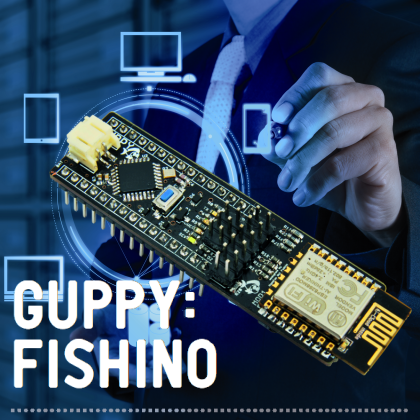
As we anticipated in the article in which we presented our Fishino MEGA (a board that is compatible with Arduino MEGA, and that is characterized by a great number of I/Os and much more program memory and/or RAM with respect to the UNO version) we have developed a board that may be considered as the other side of the coin, since it is the most essential version in the Fishino’s “saga”. It is Fishino Guppy: the name comes from the small fish – well known to those who are passionate about fish tanks- and we chose it because of the very limited size of the board, indeed the smallest Fishino. In spite of the fact that it is the most miniaturized version (as Nano for Arduino) our small Guppy shows remarkable functions and features (as you may see from the box in the next page). The peripherals that are included in the board are the ones of Fishino UNO and MEGA, with the exception of the RTC module, that cannot physically find place in the PCB, supposed to be the smallest possible. In comparison to Fishino UNO, however, we added the whole power supply stage, using a switching technology, and the possibility to power the board with a lithium polymer battery, which is an extremely interesting thing, since it is well suited for portable projects, or even wearable ones.
Circuit diagram
Let’s move on now on to the description of the circuit diagram, that may be considered as divided in the following blocks:
- power supply stage;
- battery charger stage;
- USB interface;
- Atmega328p controller;
- level converters;
- WiFi module;
- microSD-Card connector.
Circuit diagram
Since – exception made for the first two blocks (the power supply stage and the battery charger) – Guppy’s circuit diagram is very similar, if not identical to the one we already presented for the Fishino UNO board, we will limit ourselves to describe in detail the first two stages only, and will give a brief explanation for the remaining ones, and highlighting the differences with respect to the previous boards.
The circuit diagram we will refer in this description is the one illustrated in the opposite page.

The power supply
Differently from what has been done with the Fishino MEGA, in Guppy we didn’t use a Sepic stage: even if it enables us to save a component and to power the circuit on the VIN pin with a minimum voltage of 3.5 V, it proved to be too unstable because of the reduced size of the board.
In the very first prototype we had in fact used the said type, joined to a 2-layer PCB; everything worked perfectly until we started to use the WiFi module, after that the disturbances created by the latter “re-entered” the power supply’s feedback, thus causing instability.
We therefore reversed our decision, thus opting for a double converter: a step-up one for the battery input and a step-down one for the power source from the VIN input. In order to avoid the possible instability with these types, however, we opted then for a 4-layer PCB, with internal ground planes and power supply, so to create a barrier that prevents the strong pulse signals to transmit their interferences through the same printed circuit board.
With these precautions, our Guppy has therefore become extremely stable, even though the price to be paid is the one of not being able to self construct the board in the handmade way; however we have published the circuit diagram and the assembly plan anyway, in order to allow you to master the board’s hardware.

Let’s start the decription from the step-up section, that is composed by XYSEMI’s XR1151 integrated circuit, a component that has been purposely designed in order to create some DC/DC boost converters that are capable of operating with a minimal internal voltage of 1.6 V and to supply an output of 5 V with a 800 mA current, if powered with an input of 3.3 V. It is therefore optimal to accept a power supply from a common LiPo 1s (3.7 V, thus a single cell one) battery.
The integrated circuit contains all the necessary stages internally: a PWM generator, a CMOS switch with an extremely low Rdson resistor (typically 100 milliohms), the needed feedback circuitry in order to keep the output voltage stable, and a progressive start system (soft-start), used so to avoid excessive current peaks in the components that are assigned to the commutation of the output current.
The integrated circuit operates at the typical frequency of 1.2 MHz and therefore allows the usage of components (inductor and capacitors) of extremely limited size. It operates in an asynchronous way, therefore it requires an external commutation diode (D12) that in our case is a Schottky with a very low direct voltage, so to avoid hindering the efficiency.
The feedback circuitry is calibrated for a voltage of 0.6 V, the control voltage is obtained from the voltage divider, composed of the precision resistors R29 and R30, and applied to the FB input. The output potential difference is stabilized on the value given by the following formula:
![]()
The voltage is directly brought to the line of the 5 V, without any additional diode, since the D8 diode and the switch that is internal to the integrated circuit (that may be deactivated by means of the EN input of the same, on the subject of which we will return later) are already there.
A note: the XR1151 has been manufactured for operations at very low voltages, and therefore it gets damaged if more than 6 V are applied as an input; this differentiates it from the component used in Fishino MEGA’s SEPIC stage, that could accept much higher voltages as an input. It must be absolutely avoided, therefore, to apply voltages that are greater than the 5÷5,5 V at the battery input, otherwise the component and what is powered by it shall be destroyed.
We will go on with the step-down section, that revolves around Alpha&Omega Semiconductor’s AOZ1280 integrated circuit; this component accepts input voltages from 3 V and up to 26 V, and is capable of supplying a minimal output of 0.8 V. The operating frequency is a very high one, 1.5 MhZ, therefore even here we may only use components having an extremely limited size. As we could see for the case of the step-up section, the AOZ1280 contains all the components needed in order to create an asynchronous buck converter, but it requires an external block diode, signed as D11 in the circuit diagram.
The integrated circuit has a compensation input that, by means of C12, the 10 nF capacitor, enables the stabilization of the feedback network in all the loading conditions.
The EN (enable) input is not used in this case, and that is the reason why we connected it directly to the input voltage, which enables the converter as soon as it is powered.
The feedback input (FB, that is, feedback) in this case has been calculated for an internal reference voltage equal to 0.8 V; the output voltage therefore turns out to be equal to:
![]()
The Vout has been intentionally chosen as being slightly greater than 5 V, so to compensate the fall on the Schottky diode in the D10 output, that is around 0,2÷0,3 V; the said diode is indispensable, in order to avoid that the voltage coming from the step-up converter re-enters the component and goes to affect the VIN input.
Having said this, let’s go to analyze the commutation section of the power supply inputs, that is different in comparison to the diagram of the other Fishinos; it revolves around the two Schottky diodes, D4 and D5, the N channel MOSFET, Q1, and the resistors, R12 and R26. Without any voltage on the VIN or USBVCC inputs, Q1’s gate is kept at ground by means of the R12 resistor, thus switching off the component. Its output is therefore free to fluctuate and is kept at a level that is close to the power supply by the U3 integrated battery charger (that we will see later); the XR1151’s EN (enable) input will therefore find itself at a high level (via the R26 resistor) and will thus start functioning. The 5 V output will not be able to re-enter on the VIN or USBVCC pins because of the presence of the D6 or D10 diodes.
On the other hand, by applying a voltage on one of the inputs, VIN or USBVCC, the Q1 MOSFET will be positively polarized by means of the D4 or D5 diode and will therefore start conducting, bringing the XR1151’s EN input to ground and switching it off.

If the voltage at the VIN input is lesser than about 6 volts, at the output of the step-down converter there will be a voltage smaller than 5 volts, which will make the D6 diode start conducting, thus activating the power supply via USB; on the other hand, if we apply enough voltage on the VINs, the AOZ1280 buck converter’s output will be enough to bring the D6 diode to interdiction and therefore to deactivate even the power supply from the USB port.
We have therefore obtained a completely automatic commutation of the power supply voltages, like this: if a voltage is found on the VIN or on the USB plug, the battery will be disconnected from the circuit and its charge will be activated at the same time, as we will see later.
If no external voltage is found, the battery will spring into action and, at the same time, the charging circuit will be deactivated.
The last but not least important component: we will now analyze the 3.3 V regulator, that supplies voltage to the WiFi module and to the microSD card module. For the lack of space, this part ofthe circuit has been created by means of an usual linear regulator, but one having a capacity that is greater than the one in Arduino Nano; it is in fact capable of supplying a current with more than 800 mA, against the peak of 500 mA of Nano’s original voltage regulator.
Battery charger stage
This stage revolves around the very well known MCP73831 (U3); we already dealt with it in various projects and therefore we will not explain it again. The only noteworthy part is the charging activation circuit that depends on some components we already saw in the paragraph concerning the power supply’s commutation: Q1, D4, D5 and R12.
We could already see, in fact, that when a voltage of an external power supply is found on VIN or USBVCC, the Q1 MOSFET is brought to conduction and therefore its drain finds itself connected to ground. This, in addition to turning off the XR1151 step-up (as previously seen), connects the R10 resistor to ground (eventually with the R11 in parallel, if the 500 mA recharge is chosen), thus activating the recharge.
The red CHARGE LED diode is turned on during the recharge and is turned off when it is complete, if lacking the battery or if the battery charger is deactivated.
USB interface
Guppy’s USB interface stage is identical to the one used on the Fishino UNO and Fishino Mega boards, and revolves around the now well known CH340G, an integrated circuit that is capable of creating a complete USB/Serial converter with all the relative control signals, of which we only use the data channels (RX and TX) and the DTR signal for Fishino Guppy’s autoreset when it is programmed from the PC, by means of Arduino IDE.
For the lack of space, we didn’t consider here the possibility to deactivate the autoreset, a function that however is almost never used.
For a more detailed description of this module, we refer to the corresponding article in which we published Fishino UNO’s project, where it has been described in detail here.

microcontroller
This stage turns out to be essentially identical to the one in the Fishino UNO board and it uses the same microcontroller, that is to say the ATmega328P; it differs for the usage of two additional analog inputs, that is to say A5 and A6, that are not found in “UNO”s layout. As for the rest: no modification has been introduced, therefore even in this case we refer to the detailed description that may be found in the article describing Fishino UNO.
Just a note concerning the bootloader: even though this is a board that is compatible with Arduino Nano, we preferred to install Arduino UNO’s bootloader, for the simple reason that the latter occupies 1.5 kByte less Flash memory and therefore allows to load sketches having a bigger size, with respect to what is possible with Nano’s bootloade.
Therefore it is needed – while in the IDE – to select Arduino UNO as a board (and not Arduino Nano), otherwise the IDE won’t recognize the product.
In the unlikely possibility that full compatibility is required even on the bootloader’s side, it is however possible to load Arduino Nano’s original bootloader on Guppy.
Please pay attention to the ISP connector’s pinout, that in Guppy is “overturned” in comparison to the one in UNO; this has been made in order follow the original Arduino Nano’s pinout. We are informing you about this since it has already happened to the writer to “burn” a Nano board for having connected the connector in the opposite way; therefore – in case of doubt – we advise to check the circuit diagram and the PCB’s layout before executing the bootloader’s programming!
Level converter stage
Even in this stage there is no modification in comparison to the previous Fishino boards, exception made for the resistors’ value (from R13 to R23) that has been halved with respect to the one in the corresponding resistors in Fishino UNO and Fishino MEGA, so to assure a greater immunity to disturbances; such a requirement has been imposed by the extremely limited size of the board.
A greater immunity from external disturbances corresponds in fact to a lesser impedance, at the price of a small increase in the consumption during the functioning of the Wifi or of the microSD card, an increase that is anyway completely negligible. For a detailed description of the functioning, even here we refer you to the article concerning Fishino UNO; here we will only indicate that the stages are composed of resistive voltage dividers that reduce the maximum value of the output voltage from the ATmega, from 5 V to about 3.3 V, so to not damage the components that are at a lower voltage; in the opposite direction there is no need for any translation, as the 3.3 V are capable of directly driving the 5 V logics (given that the pins are 5V-tolerant).
WiFi module
As in Fishino UNO and Fishino MEGA, the wireles interface section revolves around the ESP12-F module (the last entry in the 12 series), that is based on the ESP8266 WiFi chip; the peculiarity of the module we used here is that is has a firmware that has been purposely studied in order to communicate with the Atmega328 via SPI interface, that performs much better than the serial (that the factory firmware expects to be used as for the interface). At the end of the article we will refer the substitution process of the said firmware with what is needed for the communication on SPI (the procedure is anyway on the project’s reference website. More details concerning the WiFi module are found in the articles dedicated to Fishino UNO and Fishino MEGA.
Connector for the microSD module
Even as for this stage nothing has been modified, with respect to Fishino MEGA and Fishino UNO, therefore we refer those who wanted to examine its functioning in depth to the articles concerning the said boards.
WiFi module’s firmware
update
As with the previous models, we suggest to execute a firmware update when first using the product (and to do it periodically, anyway), since it is a program that is continuously developed and closely connected to the supplied libraries. The update procedure is essentially identical to the one in the previous Fishino models: the connections to be made differ, and they are illustrated in figure The update procedure is simplified by a dedicated program, that is available for both the Windows and the Linux platforms, and it executes the operation in a completely automatic and error-free way.
The steps to be made for the update are the following ones.
- Please load a sketch that does not use the serial port. BLINK, the basic example (the one making the LED flash on the board) is perfect for the purpose. This passage is needed in order to avoid disturbances between the loaded sketch and the serial connection between the ATmega and the ESP. If the flashing program does not detect Fishino, it is 99% likely that it depends on a wrong sketch being loaded.
- Please connect Fishino Guppy’s TX port to the ESP-TX port on the ESP connector, and Fishino Guppy’s RX port to the ESP-RX port on the ESP connector
3.Please connect the GPIO0 port to ground, by means of a small cable or a bridge, and still to the ESP connector (see figure aside).
- Please connect Guppy to the PC (or press the RESET button, if it is already connected).
5.Please launch the FishinoFlasher program, and make sure that the PC is connected to the Internet.

If the connections have been correctly carried out, the program will detect the port to which Guppy has been connected, and will determine the model and the firmware version currently installed; it will connect to a remote server and will download the list of the available firmwares; the latest one will be shown and it will be anyway possible to select the previous versions, in the case you wanted to carry out a downgrade. By clicking on the “Flash” button, the update procedure will be started, at the end of it a confirmation message will appear. In order to exit the program, you need to click the “Exit” button.
In the case Guppy is not automatically detected, it is possible to try to manually select the port. It is however possible that some mistakes have been made with the connections.
The manual selection turns out to be indispensable in the rare case that two or more Fishinos are connected to the PC at the same time, in that case the first one is automatically detected, but it is still possible to select another one.
Once the procedure has been completed, it is sufficient to remove the three connections and Fishino will be ready fo the usage with the new firmware.
Well, we finished: you are now ready to develop your own applications with Guppy!

TECHNICAL FEATURES
100% compatible with Arduino Nano
WiFi module on board
Connector for the microSD module on board
Triple power supply: LiPo battery, USB port and external power supply connector (6,5÷20 volt)
Switching power supply stage with high efficiency, having a step-up converter in order to obtain the 5 V from the battery, and a step-down one in order to obtain them from the external input,
3.3 V section that has been enhanced, in order to manage the WiFi module, the microSD and possible further external components
Battery charger on board, with an indication of the charge status
From Openstore

[…] therefore a size format just barely bigger than Arduino Nano and, in terms of length, smaller than Fishino GUPPY, although it has a respectable array of built-in peripherals. We are in fact talking about a board […]