
A small integrated SMD gives life to an excellent portable FM stereo radio receiver which can be easily created because it does not require the production of coils or the calibration of tuned circuits.
The semiconductor industry continuously churns out new integrated circuits for all application areas and also for consumers and audio; among these, ICs capable of creating equipment that once required more integrated dedicated to individual stages and many electronic components. Examples we see in the progress that involved the radio receivers, once realized with transistors and at a later time facilitated by the availability of integrated devices that each implemented a stage: antenna amplifier and front-end, superheterodyne (local oscillator and mixer) frequency conversion AF like the famous SO-42P from Siemens), medium frequency amplifier and demodulator
(for example, the Philips TDA1200 or the LM3089 of the former National Semiconductors), FM stereo decoder (when required) like the Motorola MC13010P and output amplifier. Today we have integrated devices able to perform the tasks of all these components on their own and, moreover, without requiring the creation and calibration of local oscillator antenna coils, which were once a real obstacle, both due to the availability of the adjustable ferrite cores, both for the critical issues related to respecting the shape of the reels themselves, to be realized with enamelled or silver-plated copper wire.
In truth, single-chip FM radios had existed since the time of the innovative TDA7000 introduced by Philips some thirty years ago, but they still required the production of reels. Instead, for some time now there have been available components capable of performing everything internally and tuning radio signals, requiring at most quartz or a ceramic resonator and a discrete inductance or on PCB.
An example is the Hex3653, a custom in SMD encapsulated in an SOP container with 8 feet per side, used in many miniature radio receivers and in ready-made cards that are on the market.
In these pages, we propose the project of a digitally controlled FM stereo receiver, realized with this integrated circuit and powered by two simple stylus batteries, therefore suitable for portable low consumption devices.
ELECTRICAL PLAN
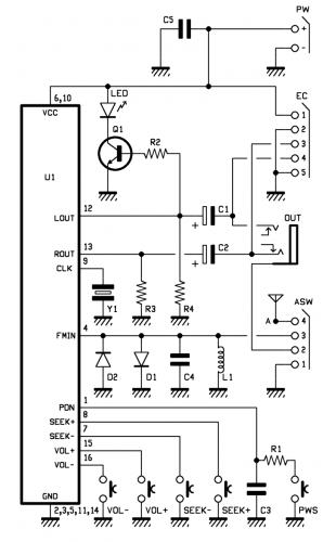
So let’s take a look at the circuit diagram, which appears very simple, since almost everything is “completed” within the integrated U1, or Hex3653; in fact we find very few external components (Fig. 1), which are the load resistances of the audio outputs R3 and R4, their decoupling capacitors (the electrolytes C1 and C2), the quartz that provides the clock for the internal stages of the chip (Y1) and the transistor Q1, used to drive the LED through the R2 resistor, in order to obtain a sort of peak meter that indicates the level of the audio signal (the more intensely the LED pulses, the higher the signal level).
In truth, the LED acts as both a power-on light (because the base of the Q1 is polarized even in the absence of a signal by virtue of the continuous component present on the LOUT output of the integrated circuit) that gives a signal meter, given that the audio fluctuations involve a change in the base polarization of the transistor.
In the circuit we also have a series of normally open buttons terminating in mass, read directly from the lines of the U1 that internally have a pull-up resistor; these buttons allow the volume to be adjusted (the VOL- and VOL + pair, which intuitively lower and raise the sound level to the stereo outputs by one step for each press, respectively), SEEK- and SEEK + for station search (the first returns back of one step, that is typically 50 kHz, at each pressure, while the second also advances the tuning at each press) and finally PWS, which allows to switch the device on or to standby. The complete scan takes less than 5 seconds.
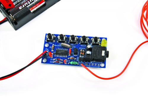
Fig. 1
Standby is a condition that allows the integrated Hex3653 to be put to sleep so that, while remaining fed between pins 6-10 and ground (2, 3, 5, 11, 14), it absorbs a current of only 10 microamps, which does not significantly affect battery life.
The PWS button is, in fact, connected to the PDN line, which corresponds to the integrated power down; note that the on / off switch is connected to the PDN pin via a resistor and that PDN has a capacitor in parallel, to ensure that the ignition signal is reliable and does not suffer from the bounce of the button contact. In fact, R1 creates, with C3, a time constant (100 kohm x 100 nF = 0.01 seconds) that allows bringing pin 1 of the integrated only if the button is actually closed for a certain time and not to make it switch if the contact is uncertain.
The tuning ranges between 76 and 108 MHz in steps of typically 50 kHz, which is the distance between the channels in “narrow” FM (in FM, normally the step between the channels amounts to 75 kHz); the extension of the tuneable FM band has been designed to cover all the frequency-modulated radio bands in the world. In Italy and generally in Europe the FM range typically ranges between 87.6 and 108 MHz.
The antenna stage of the circuit is extremely simplified and we do not find the traditional varicap diodes or the more traditional variable capacitors, but rather a fixed anti-resonant circuit; the stage in question is connected to the pin-strip shown in the wiring plan, ASW: the RF input line of the integrated unit is connected to contact 3, which, connected by a jumper with a 2.54 mm pitch to pin 4, connects it to the antenna pitch itself (typically a piece of copper wire with sheath, about eighty centimetres long). In parallel to the antenna input (FMIN pin, or 4 of the Hex3653) there is a pair of diodes connected in antiparallel, which serves to protect the chip from any electrical discharges picked up by the antenna or introduced by mistake by the wiring (it can happen if you use an external antenna connected with a coaxial cable to the wall socket in your house) as well as a very simple anti-resonant circuit formed by the capacitor C4 and the inductance L1; being the latter of 10 µH and C4 of 33 pF, the resulting band centre frequency (excluding the parasitic components) is about 87 MHz.
The tuneable signal falls in a fairly wide band since in reality this value is altered by the integrated circuit of the input and by the fact that we are in the presence of a low Q anti-resonant circuit, given that the inductance is low Q and the U1 front-end has a non-negligible load resistance.
The signal that passes within the band is then amplified inside the chip, tuned and converted by a superheterodyne circuit synchronized by the quartz Y1, then demodulated in frequency until obtaining the audio signal; the AGC (automatic volume control) stage allows the audio level to be stabilized, preventing it from being affected by the strength of the antenna radio signal. A special FM stereo decoder stage that completes the integrated, extracts the signals of the two channels, which are then preamplified and sent to the LOUT and ROUT outputs referred to the common mass. The two reach, through the decoupling capacitors C1 and C5, the 3.5 mm stereo jack connector for listening in headphones and also the EC pin-strip, which allows connection to an external stereo audio amplifier. The same EC connector allows the main power to be taken to the outside since it is parallel to the + and – PW contacts, to which the battery voltage is applied.
On the subject of audio outputs, it is worth explaining the role of the ASW pin-strip, because having among its connections both the common headphone jack and the antenna, one might wonder what connection there may be. Well, the concept is that the circuit, being born as a portable stereo radio, can use as an antenna both the headphone or earphone wire (exactly as it happens with the FM radio built into mobile phones and smartphones) and a separate antenna, be it wire or stylus, that is, of another kind; if you want to use the headphone wire, which allows you to avoid the encumbrance of the antenna, you need to jump contacts 2 and 3, which brings the common contact of the jack on the antenna input. Now two considerations must be made: the first is that the mass connection is used since in the coaxial cables for headphones or earphones is the screen and therefore the outer wire; if a signal wire were used, it would be shielded by the screen mesh and would not be able to pick up the radio signal. The second consideration is that as far as one could think that lifting the common of the jack from mass prevents the operation in stereo, in reality, it is possible and it is guaranteed because the inductance of 10 µH to the audio frequencies is practically a short circuit (the impedance that it presents at 10 kHz is just 62.8 hundredths of an ohm, against a few tens of ohms impedance of the earphones) and therefore it is as if the common was actually grounded. The same would continue to be the case.
If the wire antenna is used, the point 3 must be jumped with the 4 (thus joining the antenna pad with the FMIN pin of the integrated) and the 1 with the 2 (thus connecting the common of the stereo jack).
If you plan to integrate the radio receiver in another device containing an audio amplifier, or to connect the circuit to a stereo amplifier that allows listening in the loudspeaker, you can also not bridge the ASW contact 2 neither with the ground nor with the antenna input, because you will not use it, unless you also want to have a headphone output..
We conclude the description of the circuit with the power supply, which is filtered by the C5 capacitor and which can be supplied by a pair of series batteries, or by a lithium-ion cell or lithium polymer cell; the absorption is quite contained and at 3 volts it does not exceed 30 milliamps with a stereo headphone connected to the OUT jack.

From openstore
HEX3653 FM 76-108 MHz Radio Receiver

Really enjoyed reading this thoughtful overview; it sparks genuine curiosity right away. The way concepts build feels natural, and the practical tone keeps things approachable. Discussions around Integrated Circuits tie theory to real devices we use daily, which makes learning stick better. Overall, it’s engaging, informative, and motivating, especially for anyone exploring electronics with fresh eyes and growing confidence. It encourages curiosity, practice, and thoughtful questions from beginners everywhere today.