
Let’s start using our IoT boards based on Arduino architecture.
In our previous posts, we presented Antennino, a special Arduino board with connectivity functionalities, capable of operating in Peripheral or Gateway mode. We stopped at the hardware description and configuration, promising to return to the topic to show you an example of use applicable to the real world. We highlighted the peculiarities of Antennino, explained what Fusebits are and how to configure them, moving on to how to load a bootloader on Antennino. Now it’s time to move on to practice, enabling the communication between two modules: one configured as a remote sensor (Peripheral) and the other as a Gateway; the latter will come with the OLED display while the other will act as a sensor node.
For the latter we will use two different configurations of Antennino and consequently two sketches: the first will use the LowPower mode associated with the use of the TPL5110 chip, then, during the resting period of the sensor node, the only chip that will remain active will be the TPL5110, thus lowering the absorption to 29 nA. For the second example, we’ll use instead of the second LowPower mode of Antennino, the one specific to ATmega328P.
Then we’ll conclude by executing the OTA update of the Antennino modules.
[bctt tweet=”Let’s start using our IoT boards based on Arduino architecture.” username=”OpenElectronics”]
Let’s load the first sketch
Antennino, unlike the Arduino boards we usually see, doesn’t have a USB connector. Therefore, to be able to program it, you should already have a USB / TTL adapter. The adapter must have a female micro or mini USB connector and a 2.54 mm pitch connector with the classic pin-out [GND-CTS-VCC-TX-RX-RTS]. If possible, choose adapters that adopt the FT232 chip.
When you first connect it to your PC’s USB port you will be prompted to install the drivers. You can obtain them from the adapter vendor’s website or from the chip manufacturer.
In case you have chosen an adapter with FT232 chip, you can find the drivers in the FTDI site.
You can find alto the guide for driver installation.
Please use the USB/Serial converter.
Once the installation is complete, if you did everything correctly you should find a new virtual COM port ready for use.
Warning: before connecting the adapter to Antennino you should verify if the adapter is configured to work with a voltage of 3.3V, not 5V.
Hello Antennino
It’s always nice to receive a little instant gratification, so let’s do this: being Antennino a fully-fledged Arduino, let’s see if the classic Sketch Blink works on our two boards (Listing 1). Just be careful and remember to define the PIN associated with the LED correctly. Don’t forget, the LED is on PIN 9.
listing1
#define LED 9
void setup() {
pinMode(LED, OUTPUT);
}
void loop() {
digitalWrite(LED, HIGH);
delay(1000);
digitalWrite(LED, LOW);
delay(1000);
}
In order to start programming with Antennino, we have to specify to the IDE of Arduino which Board we are using. Antennino is compatible with Arduino / Genuino Uno, so let’s select (Fig. 1)
Tools > Board> “Arduino / Genuino Uno” from the menu. It’s not mandatory to remove the batteries before loading the Sketches on Antennino, but it’s a recommended procedure since it helps to avoid any problems in case of a wrong configuration of the jumpers.

Fig. 1
To program the board, it’s necessary to set the jumpers as shown in Fig. 2, so that you can power Antennino from the USB adapter cable.

Fig. 2
As a result, the board is powered via the linear regulator MCP1703. Regarding the pin assignment of the programming connector, refer to Fig. 3. The pin arrangement is designed so that a possible inversion doesn’t create any damages, but it’s always a good idea to pay the utmost attention when connecting the connectors. Please refer to this configuration for loading the other sketches over the course of the article.

Fig. 3
Finally, connect the USB adapter to the PC and Antennino connector and click on the button in the form of the Play IDE to compile and upload our first Sketch on our Board.
If everything is working properly you should see the LED on the USB adapter flash quickly and at the end, if there were no errors, the LED on board of Antennino should start flashing at the rate of about one pulse per second.
Well, now that we have tested our boards we can focus on something more challenging and rewarding.
We’re ready to get serious…
As you may have noticed, in the Sketch Blink we have just loaded no particular libraries have been defined.
The sketches that we’re going to use employ libraries that aren’t normally found in standard installations. We’ll need to download them, unpack them and insert them in the appropriate library folder of the IDE of Arduino.
There’s actually another way to download the libraries, but let’s use this manual practice for now: it will give us more awareness about the destination of the downloaded libraries.
In case you already have one or more of the below libraries, try to use those and replace them with the ones we suggest only in case any problem arises from the use of “old” libraries.
Let’s download these libraries:
SPIFlash
OneWire
Arduino Temperature Control
PinChangeInt
u8glib
For your convenience, libraries and source files are available in our repository.
Something that could be trivial for the more experienced but that often makes newbies waste a lot of time: after clicking the Github link for the first library, we’ll land in a page similar to the one shown in (Fig. 4).
At this point, we will have to click on the “Clone or download” button to download the library.

Fig. 4
- Unzip the file. The file will contain a folder with the following name (in this case): SPIFlash-master.
- Remove the “-master” suffix, leaving only the first part of the folder name: SPIFlash.
- Repeat the same procedure for the subsequent libraries. At this point, we have several distinct folders: RFM69, SPIFlash, etc.
- Now we need to identify where the Arduino IDE stores libraries. Normally the folder is in the following path: C:\Program Files (x86)\Arduino\libraries
- We’ll then insert the folders of the new libraries into the Arduino libraries folder. Let’s restart the Arduino IDE and we’ll be ready to work.
First test: NODE Lowpower-TPL5110 MODE
In this first test, we’ll use an Antennino board and we’ll load the Sketch Node-TPL5110.ino there. In Fig. 5 we can see how we’ll configure the jumpers once the firmware has been loaded.

Fig. 5
The corresponding sketches are quite long so we won’t report them in full on here, but we will highlight the main features;
After the initial part, we have learned the definition of two very important parameters regarding the possibility of updating the module remotely. See Listing 2.
Listing2
byte FAMILY =1;
byte FIRMWAREVERSION = 1;
byte NODEID = 1;
byte NETWORKID = 1;
byte DATA_GATEWAY_ID = 253;
byte OTA_GATEWAY_ID = 254;
FAMILY specifies the type of node. While FIRMWAREVERSION defines the current version of the firmware loaded on the node. We’ll then look at how this information is used for the OTA update.
Part of all the sketches that we are going to use from now on is the configuration of the RF section that must be customized in the value of the NODEID. In the sensor node, we are going to use we have set the value as shown in the listing. Also from Listing 2, we have reported the four main variables that define the node’s network settings.
These parameters will be loaded into the EEPROM of the ATMEGA328p chip to prevent them from being overwritten by the OTA update. The update will then modify the functioning of the node but not the network parameters of the node in order to preserve its identity on the network.
The sketch of the sensor node is structured in a classical way, with an initial part in which the import are defined, the global variables and some functions that are used repeatedly: ReadLux (), ReadBatteryLevel (), ReadTrigger (), sendData () etc. Of course, we have the part comprising the Setup which initializes the operation and the Loop cycle which is repeated until the device is reset.
Particular attention should be paid to the ReadTrigger () function that we report in full in Listing 3.
Listing3
int ReadTrigger(){
// Leggo la tensione presente sulla capacità C1
int v = analogRead(TRIGGER_INPUT);
delay(50);
// Scarico il condensatore portando il PIN in modalità OUTPUT
// e poi ad un livello Basso
pinMode(TRIGGER_INPUT, OUTPUT);
digitalWrite(TRIGGER_INPUT, LOW);
return v;
}
Let’s remember briefly that in the Lowpower mode using the TPL5110 the microcontroller is not powered and therefore the classic interrupt doesn’t work. Furthermore, it’s not enough to wake up the Microcontroller, it’s also necessary to inform it that the awakening has been caused by an alarm signal that must be intercepted by the code upon awakening. This is where the ReadTrigger () function comes into play. This function is used during the Antennino setup phase. Antennino normally wakes up according to the setting of the trimmer connected to the timer TPL5110 but this programmed wake up serves to notify the gateway that the node is still “in good health” and to send some information such as battery status, brightness etc … So the programmed wake-up should not trigger an alarm on the Gateway. If therefore the awakening is due to a scheduled event, the value read by the ReadTrigger () function will be a very low value if not exactly 0. If the sensor node awakening has been caused by bringing the WUP pin to ground, this will cause an immediate awakening of the TPL5110 even if the programmed time has not expired and at the same time the capacitor C1 charging, being connected to a high impedance analog input, will remain charged for a certain time and certainly when the ReadTrigger () function will read the value it will find it to be higher than normal and this will allow us to understand that the awakening was caused by an alarm situation.
After the analog reading of the capacity value, the PIN mode is modified and set to PIN as OUTPUT at the LOW value. This triggers the almost immediate discharge of the capacity in order to avoid finding a high value in the next awakening, due to the residual charge in the C1 capacity.
Following the discovery of a high value of the charge of capacity C1, in the Loop phase, the value of the payload structure is loaded with the alarm value = 1, with the other values acquired by the sensors and a data packet is immediately sent to the Gateway_Data. From the code extract of Listing 4 we see that sending is invoked via the radio.sendWithRetry function, which expects an ACK (feedback signal) from the Gateway node, if the node does not respond, subsequent attempts are made. When replying, the code digitalWrite (DONE_TASK, HIGH); Port High the pin Done of the timer TPL5110 which as a result of this determines the immediate removal of the voltage to the Microcontroller and the cycle repeats waiting for the expiration of the timer time or an alarm event on the awakening pin.
Listing 4
if (radio.sendWithRetry(GATEWAYID, (const void*)(&theData), sizeof(theData) , ACK_TIME)) {
Serial.println(“ -> Reply OK!”);
packet_sent_correctly = true;
Serial.println(F(“--STOP TASK--”));
// Disabilito l’alimentazione
digitalWrite(DONE_TASK ,HIGH);
}else {
Serial.println(“ -> NO reply...”);
number_of_attempts = number_of_attempts +1;
}
In the examples we used a data structure called “struct“, see Listing 5 which will be used to contain the Payload (useful load), ie the information to be sent to the gateway.
This data structure is defined in a separate MyTypes.h file that must be placed in the main sketch folder and must be included in the sketch itself using the #include “MyTypes.h” instruction. Then we’ll note that the same file actually contains another data structure that will be used for OTA programming.
Listing 5
typedef struct {
unsigned long uptime;
float temp;
float battery_level;
int lux;
int allarm;
} Payload_t;
A note on the TPL5110 chip: changing the value of the trimmer to reflect on a change in the time interval requires restarting the power supply.
Second test: Node Lowpower-ATMega328P mode
In this second exercise, we’ll use an Antennino board in Lowpower mode. In Fig. 6 we can see how we’ll configure the jumpers once the firmware has been loaded. In this case, we’ll load the Sketch Node-LowPower.ino.

Fig. 6
We’ll analyze only the most interesting parts of this Sketch. In Listing 6 we see a part of the loop and in particular, the management of the passage in LowPower mode, the interception of an interrupt alarm and the sending of a periodic information packet to the Gateway_Data.
listing 6
if (TriggerDetected) {
batteryReportCycles =0;
TriggerStatus = digitalRead(TRIGGER_INPUT);
sendData();
Blink(LED,3);
} else if (batteryReportCycles >= BATT_CYCLES) {
// invio le notifiche sullo stato della batteria solo se sono in modalità LowPower
if ( Sleep_Time > 0 ) {
sendData();
Blink(LED,3);
}
batteryReportCycles=0;
}
if (Sleep_Time >0) {
for (byte i=0; i < Sleep_Time; i++) {
LowPower.powerDown(SLEEP_8S, ADC_OFF, BOD_OFF);
}
}
batteryReportCycles++;
Note that if an interrupt is intercepted, the TriggerDetected variable is set to true in the loop and this determines the sending of information to the Gateway_Data via the sendData () function, which sends the data structure Payload_t evaluated with the data received from the sensors and the status alarm. If there are no alarms during the normal execution, then the sending of data happens when batteryReportCycles >= BATT_CYCLES, for each call, the variable batteryReportsCycles gets increased and, when it reaches the value of BATT_CYCLES, a data pack is sent toward Gateway_Data.
The time-out condition is the function LowPower.powerDown which allows us to bring the microcontroller to a low power state for 8 seconds.
It’s possible to overcome this limit of 8 seconds by including the function in a loop, as seen in Fig. 7.

Fig. 7
In this case, if Sleep_Time = 1 the time-out condition is set on 8 seconds, otherwise it will be equal to 8S * Sleep_Time.
If we set Sleep_Time = 0, the sensor will never go in a low power state.
To trigger an alarm, it is necessary to “BRING DOWN” the PIN D7.
This event will awake the node, will determine the sending of a data structure, containing the alarm value set to 1 and then the node will return in a LowPower mode.
Gateway_Data
Possessing a network of sensors without being able to process the information they collect is of little use, therefore it’s necessary to have a Gateway_Data node that acts as a concentrator for all sensor nodes. For this purpose, we must upload the Sketch Gateway_Data.ino to an Antennino module.
Like we did with other cases we’ll not report the complete listing but only the most important features.
The Gateway_Data must be able to receive the information coming from the sensor nodes, so it must refer to the data structure transmitted by the nodes, we’ll, therefore, have to include MyTypes.h (see Listing 5).
The gateway will have NODEID = 253 and therefore this id will not be used by other nodes of the network. It must be configured in all sensor nodes in the DATA_GATEWAY_ID variable.
On the module, we have provided the ability to view the data received in real time via a small OLED display.
In case we don’t want to use it, we can remove all references in the code including the import of the library and use the serial port to view the data received on the serial monitor connected to the PC.
If, on the other hand, we intend to use the Oled display, we first have to make sure that the pinout of the same is compatible with the default one of Antennino, otherwise, it will be necessary to reverse the tracks under the Oled display connector. Do not insert a display with an inverted pinout because you risk compromising the operation of the display or the controllers on Antennino.
We also need to check the chip used on the display.
There are already two options in the code:
a configuration related to the SH1106 chip and one related to the SSD1306 chip. In the absence of punctual information on the form it’s going to be trial and error, but don’t worry, nothing serious will happen: at most the display will remain black.
The Gateway_Data doesn’t allow the memorization of the information received from the sensors, therefore the ideal would be to connect the Gateway through a serial port to a Raspberry Pi, equipped with specific software that allows to historicize the received data on a dB MySql and possibly visualize them through a web interface.
This option is already in the pipeline and we’ll see if we can explain it in another article. For now, we could just intercept the arrival of an alarm from a node and activate an output pin from the Gateway connected to an alarm. We have to decide how to feed the Gateway_Data. Consider two options.
if (radio.receiveDone()){

if (radio.DATALEN == sizeof(Payload_t)) {

byte myOwnBuffer[radio.DATALEN];

memcpy(myOwnBuffer, (const void *)radio.DATA, radio.DATALEN);

Cast_To_Struct(curData , myOwnBuffer);
Using the batteries on board the module employing the Step-Up Max856 regulator. This, of course, is a test option but that makes no sense to use in a real setting (Fig. 7).
The other option uses an external power supply to be applied to the Vin pins of the Antennino module and will be brought to 3.3 V by the linear regulator MCP1703 on board the Module Fig. 8

Fig. 8
The operation of the Sketch is actually very simple: as usual, there is a section of variable definition and common functions, a setup function and a loop that intercepts the data received from sensor nodes. The following piece of code proposes the Gateway_Data Loop.
Here we manage the display of data on the display; alternatively, we can manage the reception of an alarm condition from a node, using for this purpose curData.allarm:
}else{

Serial.print(F(“Invalid payload: “));

Serial.print(‘[‘);Serial.print(radio.SENDERID, DEC);Serial.print(“] “);

for (byte i = 0; i < radio.DATALEN; i++){

Serial.print((char)radio.DATA[i]);

}

Serial.print(F(“   [RX_RSSI:”));Serial.print(radio.RSSI);Serial.print(“]”);

Serial.println(“”);

}
Analyzing the code, it’s evident that the data received by the sensor is taken into consideration only if it has a dimension that is consistent with that of the data structure that is expected Payload_t otherwise a message with the text: “Invalid payload” is issued.
If the message size satisfies this first filter, the message itself is “converted” by the Cast_To_Struct function (curData, myOwnBuffer) into the data structure that is expected, in order to extract the necessary information and then display it on the display, activate the pins or send them to a possible Raspberry pi via serial.
Firmware OTA update
During normal operation, our sensor nodes, whether using the native LowPower mode or the one associated with the TPL5110 chip, will most of the time be in low power mode and therefore will not be reachable from the Gateway.
So, it will be the sensor node to request the firmware update when it wakes up from the LowPower mode.
To implement this functionality we modified the behaviour of the RFM69_OTA.cpp library of wireless programming by adding specific functions, and we have created the Windows application AntenninoFlashProgrammer.exe
For this purpose, it’s necessary to load the Gateway_OTA.ino sketch on an Antennino module that must be dedicated to performing the function of Gateway_OTA.
The Windows application in concert with the sketch loaded on the Gateway_OTA module allows reading a binary .hex file originated from the compilation made with the Arduino IDE and to load it on the FLASH memory on board of the Gateway_OTA module.
Once this is done, the module is put into Remote Programming mode and will be able to receive update requests from the Sensor nodes that are in Lowpower mode.
If we have nodes that are always on we can directly upload the update by defining the node_id target on the interface of the Windows application and send the new firmware to the node. In this case, it is up to us to make sure that the node we have identified as the target is suitable to receive the version of the Firmware that we have ready on the Gateway_OTA node Flash.
If we were wrong, nothing serious will happen, as long as the new firmware complies with the Antennino Node standard. If by mistake we load on the Flash of the Gateway_OTA module a sketch like Blink.ino the update would take place but then it would be impossible to perform a further OTA update of the node and we would have to disassemble the node from its location and reprogram it via serial.

Fig. 9
In the case of programming Lowpower nodes, to ensure that the update takes place correctly, you can check the family membership and the current firmware version of each node.
Upon awakening, the sensor node sends an update request to the Gateway_OTA, providing the current firmware version (FIRMWAREVERSION) and the node family (FAMILY) so that the firmware is loaded on the correct type of remote nodes.
The variables relating to the Remote Node ID (NODEID), Network ID (NETWORKID), Data Gateway ID (DATA_GATEWAY_ID) and Gateway OTA (OTA_GATEWAY_ID) are saved in EEPROM, so that they are not overwritten by the Firmware update.
The gateway receives the remote update request and checks whether the firmware available is suitable for the requesting node. It makes a comparison between the requestor’s family and the one assigned to the sign on the gateway and verifies if the firmware version of the requesting node is lower than the one present on the Gateway.
If these two conditions are met, the update procedure is initiated and at the end the Sensor node is restarted. When there’s a new awakening from the Lowpower state, if the version on the gateway is not updated and therefore increased in version number, no subsequent update process will occur. To understand where Arduino saves the binary .hex files of the builds it performs, we need to enable an option in the IDE.
Let0s go under File / Preferences and check “Show Verbose Output” (Fig. 10).

Fig. 10
Then we send a sketch and compile (Fig. 11) the path in the log part of the IDE of Arduino.
In particular, we have obtained the following path:
C: \ Users \ AppData \ Local \ Temp \ arduino_build_113078 / Node-TPL5110.ino.hex

Fig. 11
Unfortunately, every time we close the IDE and reopen it to compile, the part arduino_build_XXXXX changes randomly. But we’re interested in the initial part of the route. Let’s launch the Windows Antennino Flash Programmer.exe application and open File / Settings (Fig. 12) and insert the default BaudRate (115.200) and the search path for the binary files compiled by the Arduino IDE.

Fig. 12
To test the functionality of this feature, let’s open the IDE of Arduino and send a sketch in compilation. At the end of the compilation, leaving the Arduino IDE open, launch the Antennino Flash Programmer application and click on the “File to Upload” Combo Box (Fig. 13) this will call a function that will provide us with the path of the last file as the first element binary compiled by the IDE of Arduino. Useful, right?! This will prevent us from having to read the long and verbose compilation log of the IDE every time we look for the compiled binary file.

Fig. 13
Now let’s see how to load the binary .HEX file into the Flash memory of the Gateway_OTA. We will have previously loaded the sketch Gateway_OTA.ino on the Antennino module appointed for this purpose. We connect the USB RS232 adapter to the module, select the correct port, leaving the other parameters unchanged.

Fig. 14
Click on the “Load to Local Flash” button (Fig. 14). After a few seconds a dialogue window will be shown (Fig. 15) which requires consent to upload. Selecting Yes starts the procedure to load the binary file in the Flash Memory of the Gateway_OTA.
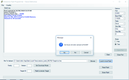
Fig. 15
After completing the procedure (Fig. 16), in order to send other commands, we have to wait for the Timeout to occur (30 seconds).

Fig. 16
At this point we can check the contents of the Flash memory (Fig. 17), then let’s clear the Application Log window by clicking on the “Clear” button.

Fig. 17
Now, let’s test the OTA update of a node. To do this, we will also need an Antennino node in addition to the Gateway_OTA node, with a sketch of a node on board, for example, TPL5110.ino. If we use the node TPL5110 we must set the jumpers as we have already seen in Fig. 5. For convenience (but it’s not essential) we could also connect the sensor node via serial to the PC (we would need two USB adapters though). Once we have connected the node to the serial we can open the Serial Monitor relative to the door to which the module is connected. At this point, we should see a Log similar to that shown in Fig.18. The node, about every 8 seconds, looks first to contact the Gateway_OTA by sending them the node family and the Firmware version. And then it also tries to send data to the Gateway_Data to update it on the status of the sensors. Now we also connect the Antennino module to the PC via USB adapter, which carries out the task of Gateway_OTA. We run the application Antennino Programmer.exe and from the board of the same, we set the Gateway_OTA in download mode (Fig. 19). We then open the serial connection to the Gateway module, insert the Firmware family and the version relating to the binary loaded in the Gateway Flash and click on the “Set Download Mode” button. As soon as done we will see the node update requests arrive and if the conditions are correct the new firmware will be downloaded and at the end, the remote node will restart with the new version.

Fig. 18
At this point, if we have kept unchanged the conditions of the Gateway we will see that to the new update requests the Gateway_OTA will reply that no update is necessary for the node because the version currently present on the remote node is the same as the one present on the Gateway.
An actuator type node can also be updated. So a node that isn’t working in LowPower mode. In this case, it is sufficient, once the Binary File of the new firmware has been loaded on the Gateway_OTA, enter the target ID of the node to be updated and click on “Flash to Remote Target”.

Fig. 19
The binary file will be sent to the remote node which, after completing the procedure, will reboot with the new version of the Firmware (Fig. 20).

Fig. 20
Conclusions
In this article, we initially loaded a test sketch and then went on to test the communication capabilities between a sensor node and a Gateway node. Then we saw how to use the remote OTA update using a specific gateway and a Windows Application that allows us to load the binary in the Gateway node Flash, and to set the update mode of the nodes. In the next issue, we’ll see how to implement a Raspberry Pi Gateway to historicize sensor information and display data on a web interface.
From openstore
Pololu USB AVR Programmer v2.1
