
On the hardware of the controller board LED Matrix, by taking advantage of the reconfigurability of the onboard FPGA, we can build a bivalent tool that is extremely useful to have on our work bench.
If you’re looking for a tool for measuring frequency that is not the classic multimeter and, in the various drawers of your lab, between a forgotten board and various devices, you can’t find one, worry not: you don’t have to spend a fortune in professional tools, because we have you covered, creating the project you can find in these pages. It is a bivalent tool, since it both acts as frequency meter and clock generator, very useful in this era where logics and digital devices are extremely commonplace. You can surely find ready-to-use tools on the market, however it makes sense to create our own: it is not based on the classic integrated circuits, oscillators, counters or microcontrollers, but on an FPGA (Field Programmable Gate Array).
And a programmable logics is also what is at the base of the Led Matrix controller board that we have proposed in the “big modular display” project presented in this post, where we stated that the same board could be reconfigured to carry out many other tasks, including a frequency meter, given the availability of BNC connections and the hardware support for frequencies revolving around 400 MHz.

Ipso facto! We turned the Led Matrix controller in a bona fide 2-in-1 lab tool: a frequency meter and clock generator. Thanks to the re-programmability of a FPGA-based system, we can develop a new project that has nothing to do with the previous one except for the fact that both share the same development board. In this case, however, the Spartan 6 FPGA will control a second board with a 12 digit display that will display the frequency value of the input signal to be measured.
The block diagram of the two boards that will be connected together through two flat cables is shown in figure. The FPGA that you can see at the center takes as input the signal to measure through the BNC (CN7) connector and generate the control signals for the 12 digit display. A second BNC (CN8) is used to generate a general-purpose clock. The Led Matrix controller board also have auxiliary components: the 27 MHz input clock as reference to synchronize the internal logics of the FPGA, a USB port that is needed to program the PROM flash memory through bootloader (which can contain up to 15 configuration images for the FPGA) and, finally, a DIP switch (DSW1) that we are going to use ask clock frequency selector provided on the tool’s output.

Circuit diagram
Now, let’s analyze the circuit diagram of the display board which contains the frequency meter display (the 12 digit display, if you prefer…) While for what concerns the more complex Led Matrix controller board, of which we are also reporting the electric diagram, we refer you to the September 2016 issue. As you can see, display control takes place in multiplex, which makes sense given the amount of lines that it would take if we had to individually control the single segments (7 besides the floating-point) of 12 elementary displays (which require 84 lines); in this mode, we parallel connect the corresponding segments of all displays (i.e. all the A’s together, all the B’s to get her etc.). Therefore, in the circuit diagram the common lines for segments of the 12 digit LED displays form a bus on which the FPGA sends out data each time destined to a specific digit; each display is turned on when the corresponding signals travel on the bus, thanks to a PNP transistor acting as a static switch, that positively closes the common anode.

In our project, the digits are grouped by 4 in three 4-digit, common-anode displays, each one predisposed for multiplex control, therefore on its pins it has terminals of the segments of the four digits, connected between corresponding segments.
In detail, the segment bus (a, b, …, g, dp) of the three 4- digit, common-anode displays (code DISPLAY4DGIALLO) are connected in parallel to the CN4 connector through a polarizing resistance in series (R1 ÷ R8). The CN1 connector of the display board is connected to the CN4 of the Led Matrix Controller board through a flat cable so that each segment is connected to a buffer of the FPGA. For instance, starting from the VHDL code (TopLevel_LED_Matrix.vhd, downloadable from our website), the internal signal “Segment_A” is connected to the port/buffer P1_RED_1, which is connected, as specified in the constraints file (TopLevel_LED_Matrix.ucf) to the 34-pin using the following instruction: NET “P1_RED_1” LOC = “P34” | DRIVE = 24 | IOSTANDARD = LVTTL.
The 34 -pin of the FPGA is directly connected to the 1-pin of CN4 connector, which will be brought, through the flat cable, to the 1-pin of CN2 connector of the display board. Said 1-pin is connected, through the series R1, to all the “A segment” LEDs of the three 4- digit displays. Each digit has, on the other hand, a dedicated driver, for instance, the PNP T12 transistor is piloted by the Digit 1 signal connected to the 1-pin of CN1 connector (CN5 of Led Matrix board) connected to the 2-pin of the correlated FPGA port P2_RED_1 connected to the internal signal Segment_MUX_Driver(0). In conclusion, only when both signals Segment_A and Segment_MUX_Driver(0) are forced to zero by the FPGA, the “a” segment of digit 1 will light up. In case we decide to use a common cathode display, we would have to use NPN transistors which emitter will be connected to ground instead of that to 5 V; in this case, the JP1 jumper that is positively closed in case of common anode on the +5V, must be connected to ground.
Up to this point, we have seen the digit lines, however there are two connections on the Led Matrix that can be used both for digital and analog signals, which can be accessed from the BNC connectors labeled CN7 and CN8; we can use it, the first one to read the frequency and the second one to send out the signal produced by the generator. The two terminals, in general, can be used interchangeably as inputs or outputs, thanks to the wide flexibility of FPGAs, it depends on the software.

The peculiarity of BNC lines is that, unlike other I/Os, are differential and are uncoupled on the Led Matrix board through signal transformers (TR1 e TR2) with central plug secondary that allowed to go electrically isolate them without altering linearity, like it would happen if we were to use, for instance, photocouplers. Besides, using transformers do not impose any thresholds and the applicable signals can also be very weak. Their processing will be carried out by the FPGA blocks selected each time by the application’s firmware. Note that the word “differential” refers to the FPGA side and not to the BNC: in fact, on the BNC side the inputs are unbalanced (refer to ground) why all the FPGA side they are balanced, i.e. they refer to two I/Os.
Each BNC is uncoupled through a capacitor connected in series to this signal wire, so that if the LED matrix board is connected to directly polarized devices, the transformer doesn’t act as load; each BNC is also connected in series to a 75 ohm resistor, which stabilizes the input impedance on that value. On the internal side, the central-plug secondary (connected to ground) provides two signals in phase opposition, each one, through series R/C dipoles (to uncouple and stabilize the impedance) is connected to a couple of I/Os of the FPGA.
HOW IT WORKS
As it is always the case when you deal with programmable logic, it is not enough to define the block diagram of the FPGA board in order to explain the hardware functioning of the project, however it is fundamental to the find the logic diagram of what we are going to implement in the FPGA. Let’s start from how we can measure frequency of an arbitrary signal. Let’s start by defining frequency, frequency represents number of cycles that a periodical vari bull amount completes within a time unit (1 second). Therefore all you have to do is count how many cycles takes place during a second in order to obtain the frequency of the signal.
Counting the cycle means, in our case, counting how many rising edges there are in a second, i.e. we have to count, within a second, the total number of transitions from 0 to 1 of the signal to be measured.
The first thing we can think about is that, in order to count the edges of the signal, we would have to have a counter that has the signal to measure as clock source. Theoretically, we could choose this kind of implementation, but we would soon have to deal with the harsh reality of a project with more clock domains, one to measure and the one synchronizes the rest of logics. For this reason, we prefer to take advantage of a solution that uses just one clock domain.
As shown in figure, let’s suppose we have an input signal to measure that is 25 MHz. The first thing to do is to “read” the input signal, i.e. we have to sample it (using an internal FPGA clock, for instance at 100 MHz) that is going to save the values of the sampled input signal in a 8-bit register. Then, we have to count, for each batch of 8 samples plus the previous sample, how many 0 – 1 transitions there are.

In the example shown in figure, the partial count for each block of 8+1 samples is equal to 2 rising edges.
Finally, we have to add all the partial counts for a total time of one second in order to obtain the number of 0 – 1 transitions of the input signal took place within one second, i.e. the frequency.
With a 100 MHz sampling frequency, the Max frequency we can correctly measure is equal to 50 MHz, that is half of the sampling frequency.
Xilinx library
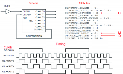
Before analyzing the block diagram, we must briefly talk about the 2 modules included into the Xilinx library: Phase Locked Loop (PLL) and Serializer-Deserializer (SerDes). The first PLL allows to generate, starting from the reference input clock, one or more output clocks with frequency values, face values and duty cycle values that can be configured through appropriate attributes. As illustrated in the example, from the input clock CLKIN1, equal to 100 MHz (as specified by the attribute CLKIN1_PERIOD=10 ns we can generate the output clock CLKOUT0, which we can see can be calculated following this formula below:
FCLKOUT0 = FCLKIN1 x M/(DxO)
That is:
100 MHz x 8/(1×2) = 400 MHz
Same thing for FCLKOUT1=400 MHz but with 90° phase, while
FCLKOUT2 = 200MHz with duty-cycle equal to 25%.
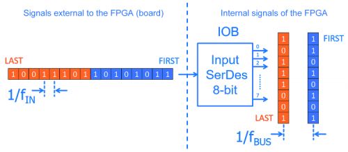
The second module, Input SerDes, located in every input-output block (IOB) of each FPGA pin, allows to turn a high-speed serial input signal in a parallel internal bus (2, 4 or 8-bit) which fBUS is equal to the frequency of the input signal fIN divided by the amplitude of the bus expressed in bits, as visually shown in figure where fBUS=fIN/8.
Block diagram
We finally have all the elements to describe the “internal” design of the FPGA that we have divided into parts for simplicity, the first block diagram is the actual frequency counter, while the second one represents the driver for the 12 inch display. The frequency counter represented in figure is divided again in four stages:
- CLOCK: starting from the input clock of the FPGA SYS_CLK_PIN (27MHz) the PLL, configured through appropriate attributes, generates the main clock CLK_DIV_IN (114,75MHz) and the high-frequency clock CLK_IN (918MHz) for sampling the input signal FASTLINK to measure;
- SERIES-PARALLEL: SerDes samples the serial signal FASTLINK through CLK_IN and generates an 8-bit parallel output which is synchronous with CLK_DIV_IN;
- EDGES COUNT: the INCREMENT_VALUE signals represents how many rising edge of the FASTLINK signal took place in each CLK_DIV_IN cycle (only if two adjacent bits have 0 value, for the least significative beat, and 1, for the most significant bit, the AND port output is 1);
- FREQUENCY CALCULATION: the difference (COUNTER_HZ) between the accumulation of INCREMENT_VALUE signal and the accumulation saved 1sec before it represents how many rising edges of FASTLINK took place within 1sec, that is to say the frequency for FASTLINK.

The display driver represented in figure is composed by 2 parts:
- BINARY TO BCD: the binary signal (COUNTER_HZ) is converted in a signal with 10 decimal digits, one for each display (for instance, suppose we have counted 162 0 – 1 transitions for the signal to measure, that is COUNTER_HZ=10100010b = 162; therefore, on display 0 we would have to display the figure BCD_Data[3:0]=2, on display 1 the figure BCD_Data[7:4]=6 and finally on display 2 the figure BCD_Data[11:8]=1, while 0 will be displayed on all the others);
- DISPLAY SELECTOR: each figure (BCD_Data[x+3:x] with x equal to 0, 4, 8, …36) must be forced to rotate (every 0,5ms) on the 7-segment bus which is common to all the displays and at the same time only one display ads time is activated through the Driver[11:0] bus corresponding to the corresponding figure.

The FPGA firmware
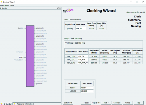
Before getting to the bitstream generation (please remember that when we talk about FPGA, the firmware is called bitstream) to configure the FPGA in the ISE development environment of Xilinx, let’s move from functional description to RTL description through the VHDL code that allows defining the behavior of the circuit in terms of signals, registers and Logix operations. As shown in figure the “TopLevel_LED_Matrix” entity is composed by four components: CLOCK_PLL (clock generation), Freq_Counter_IN (serial/parallel conversion and edges count), Frequency_Counter (frequency calculation and bin2bcd conversion), Seven_Segment_Driver (display selector). Let’s see together some crucial sections of code. The Clock_PLL entity has been generated using the Xilinx CoreGenerator utility allows to automatically configure the PLL attributes after specifying input and output frequencies as shown in the Clocking Wizard in figure. In particular, CLK_IN at 918MHz is used to sample the signal to measure, while CLK_DIV_IN = CLK_IN / 8 = 114,75MHz is the main clock controlling the entire FPGA Logix. The Freq_Counter_IN entity contains 2 4.bit SerDes inputs connected in cascade to pass from serial signal FAST_LINK_RX to 8-bit parallel bus iserdes_q, and the process “Rising edge counter” to count each clock cycles and transitions from 02 1. In List 1 we propose a code for the FPGA called Freq_Counter_IN.vhd, only the section (due to space) implementing the transitions detection.
If we take a look at the code in List 1, we can see that the 9-bit bus Edge_Detect_Array è is associated to the 8-bit bus iserdes_q, plus the previous sample. Only if they release a rising edge between two adjacent bits in Edge_Detect_Array, the corresponding Rising_Edge_x is forced to go high. Finally, Increment_Value is the sum of all the Rising_Edge_x, refresh for each clock cycle (in VHDL the operands the result of an addition must all have the same number of bits, therefore for each Rising_Edge_x we had to add 3 zeros in the most significant position). The Frequency_Counter entity receives Increment_Value in output, which is accumulated in Counter_Value as shown in List 2 (where System_Clock is equal to CLK_DIV_IN). In the same place you can find the code section Frequency_Counter.vhd, which allows to measure the input frequency, measuring the frequency based on the impulse count. Besides, every second (Gate_Time=0x06D6F22F114749999 clock cycle for a duration of 1/114.75MHz=8,71ns each, 1144749999×8,71= 0,999sec) we save the value of Counter_Value and calculate the difference between the current value and the one saved one second before, therefore obtaining Counter_Hz, which represents the number of 0/1 transitions registered in one second, i.e. the signal frequency.
List1
-- Rising edge counter
process (CLK_DIV_IN) begin
if (CLK_DIV_IN’event and CLK_DIV_IN = ‘1’) then
-- -------------------------------------------------------------
Edge_Detect_Array <= iserdes_q & Edge_Detect_Array(8); -- MSB Carry
-- -------------------------------------------------------------
if (Edge_Detect_Array(1) = ‘1’ and Edge_Detect_Array(0) = ‘0’) then
Rising_Edge_1 <= ‘1’;
else
Rising_Edge_1 <= ‘0’;
end if;
-- -------------------------------------------------------------
if (Edge_Detect_Array(2) = ‘1’ and Edge_Detect_Array(1) = ‘0’) then
Rising_Edge_2 <= ‘1’;
else
Rising_Edge_2 <= ‘0’;
end if;
-- -------------------------------------------------------------
.......
-- -------------------------------------------------------------
if (Edge_Detect_Array(8) = ‘1’ and Edge_Detect_Array(7) = ‘0’) then
Rising_Edge_8 <= ‘1’;
else
Rising_Edge_8 <= ‘0’;
end if;
-- -------------------------------------------------------------
Increment_Value <= (“000” & Rising_Edge_1) +
(“000” & Rising_Edge_2) +
(“000” & Rising_Edge_3) +
(“000” & Rising_Edge_4) +
(“000” & Rising_Edge_5) +
(“000” & Rising_Edge_6) +
(“000” & Rising_Edge_7) +
(“000” & Rising_Edge_8);
-- -------------------------------------------------------------
end if;
end process;
One last note: at the right time, you will have to power the display board through a coated (0.5 mm of diameter is enough…) wire segment onnected between +5V of the jumper of the corresponding PCB and the +V terminal of the LED Matrix controller, where you will bring the assembly power. Reference ground and power ground on the other hand, travels through the flat cables.
List2
-- -------------------------------------------------
-- Frequency counter
-- -------------------------------------------------
process (System_Clock) begin
if (System_Clock’event and System_Clock = ‘1’) then
-- -------------------------------------------------------------------------
Counter_Value <= Counter_Value + Increment_Value;
-- -------------------------------------------------------------------------
if (Gate_Counter = Gate_Time) then
Gate_Counter <= x”00000000”;
Data_Captured <= ‘1’;
Counter_Data <= Counter_Value; -- Saving previous value
Counter_Hz <= Counter_Value - Counter_Data; -- Providing Out counts
else
Gate_Counter <= Gate_Counter + 1;
Data_Captured <= ‘0’;
end if;
-- -------------------------------------------------------------------------
end if;
end process;
Uploading the firmware
The FPGA configuration is made extremely simple by a terminal emulation program called RGB Matrix Terminal, which is written for this purpose and equipped with many features, and you can see its launch screen in figure. Once launched, in the lower left section of that screen you can find the drop-down menu with the available COM ports; from that, select the one with which terminal communicates (the other one is not used in this application).

For this purpose, we remind you that the IC allowing to connect the L ED matrix board with the PC (chip FTDI FT2232HL) is a double USB/TTL converter, therefore by connecting the board to a Windows computer, two virtual COMs will be created: one refers to the control see your connection and allow us to manage the firmware loaded in the FPGA; the other virtual COM in this application is not used. Unfortunately, when working on a Windows, it is not easy to identify COM’s, therefore it is necessary to select one and press enter from a terminal; if you see the screen in figure you can proceed. If not, you have to say that the other one.

By using the dialogue window that can be accessed from the FPGA Programmer menu, we can check the firmware version that manages our lab tool (it is a file with .bin extension) and possibly update it. To do so, we have to select a slot, name it and, using the rightmost button, we are going to search for the firmware file to upload in the appropriate location (these files must be in .bin format). From the same screen you can also select (with flax) which of the uploaded firmware is will have to automatically launch when the LED matrix board is activated. After uploading the firmware we want, we can now finish our frequency meter/clock generator.
Of course, the whole bitstream selection thing makes sense if there are more than one firmware in the program memory, otherwise there will be just one and that one will be executed.

Test
Once the firmware upload is completed, disconnect the board from the DC, connect the two units using the flat cables (remember that the CN4 connector of the LED matrix controller board goes to CN2 and CN5 of the LED matrix controller board goes to CN1 of the display board) and power the LED matrix board through to two eyelet terminals; you need 5 V DC with a current of around 600 mA. In order to run a test, check if the displays turn on, then, if you have a simple signal with the frequency value ranges from 100 kHz to 4 MHz, you can use a probe with BNC connector (that you will connect to the BNC plug on the left side of the LED matrix board), touch the point (the ground crocodile clamp must be applied to the ground of the circuit generating the signal) and verify what the tool shows.
As a frequency you can also use the one you can find at the terminals of a quartz of a PC motherboard, of course, powered on, taking care not to cause any damages. Remember that the circuit accepts rectangular 0/5V or 0/3,3V TTL at standard TTL level.
We also remind you that from the right side of BNC of the LED matrix controller you can take the signal generated in the clock generator function.

As for the measurements, we must point out a couple of things: tolerance, i.e. maximum error by our tool when functioning as a frequency meter, depends on the tolerance of the onboard oscillator (IC1) that is equal to 20 ppm in our case. This means that the error is 0.02 per thousand!
As for the signal to apply to the input (we are still talking about the frequency meter function), this must be a rectangular signal with sufficiently steep rise in edges; to be specific, minimum incline allowed is 20V/µs.
Conclusions
In this article, we have seen how to visualize frequency, measured in hertz, on a 12 figure display for a periodic signal through a system based on FPGA. By reusing the LED matrix controller demoboard presented in September 2016 and take advantage of some elementary components from the Xilinx library (Input SerDes and PLL) we were able to develop a single-clock domain RTL project, capable of counting all the edges of an input signal ranges from 100 kHz to 400 MHz and at the same time, generate a 4-frequency clock signal which can be selected through a DIP switch.
From openstore
Display panel module – to be mounted

Hi!
where can I find the .bin file to load into the “LED Matrix Controller”?
Hello Mr. Landoni,I am interested in frequency meter.Could you made this frequency meter for frequencies up to 400 Mhz with resolution +-1 nano Hz? The LED display will has 18 numbers. Greetings Filip Novák
Where is the project files?