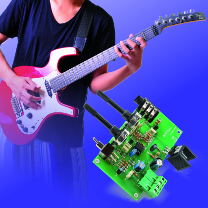
Amazing board with volume and tone controls and a distortion fuzz integrated with activated/deactivated on demand; complete with a speaker and a power supply, it constitutes an essential tool for guitar exercises.
Who likes to play electric guitar, unfortunately, knows that this instrument, unlike its acoustic alter ego, hasn’t a sound box: you can only, therefore, play only if the pickups mounted under the strings of the guitar are amplified. For this reason, exercising can become a problem, since without an amplifier you just hear a poor sound, while with the amplifier on – at least, with a conventional one used as a monitor in recording rooms or on stage – you risk a fight with your neighborhood at each chord. Practicing with an electric guitar needs a specific amplifier, that keeps intact the basic controls but that has an output power compatible with the home environment, so not too high to disturb our neighbors: a pair of watts or little more may be enough.
Hence… we present an amplifier that has these characteristics and was developed to play at home. In addition to the tone and volume controls, it integrates a distortion-type fuzz, which is a signal shearing, activated and excluded by a specific command. This type of distortion is clipping type and it is not to be confused with the throttle of the guitar, that distorts notes changing pitch as it varies during the vibration of the string, the tension of the same varying the length of the oscillations (more tension corresponds to an increase of the frequency and vice versa). The throttle distorter is a pitch control, a frequency distortion, while the fuzz is a distortion of amplitude and waveform.

Wiring Diagram
Without further ado, let’s take a look at the amplifier circuit, whose circuit diagram can be broken down into four sections: a preamplifier input, a key control, a second amplifier signal, an operational shearer and a power amplifier. Starting from the preamplifier, that provides a first amplification of the signal supplied by the pick-up of the electric guitar and that is achieved with a cascade of two stages in the N-channel JFET with common source configured with automatic polarization. Automatic polarization means that the JFET stabilizes by itself the operating point thanks to the special connection of the gate and the source; to understand how it’s working, consider that the JFET is ideally composed of a silicon finger whose extremes are headed to the drain and source terminals (those at the top and bottom aligned in graphic symbol) surrounded by a ring attached to the gate (in graphic symbol corresponds to the arrow). If the finger is doped N the ring is P-doped and vice versa; in the first case, we speak of N-channel JFET, in the second P-channel JFET. The diffusion of impurities of opposite polarity to the dopant of the finger results as a PN junction, which behaves like a diode, but that in the JFET must work in reverse or void polarization; for this reason, the resistance between gate and source or drain is theoretically infinite, so the gate could be considered isolated (it is not really, because the junction leads to a minimum current leakage when it reversed polarized). The higher the reverse polarization voltage is, the more the channel narrows, ie the part of the finger section in which there are available charges to originate and to maintain the current between drain and source. The JFET is, therefore, a sort of variable resistance controlled by a voltage.

In our circuit JFET are N-channel based, then the channel has the minimum resistance with the zero polarization and the maximum by applying the maximum permissible negative voltage between source and gate. The automatic polarization is obtained by playing on the fact that the gate theoretically does not absorb current: feeding the circuit, between the drain and source a current flows which determines a voltage drop between ground and source; by connecting the gate to ground through a resistance (which can be of high value, with a total advantage of the input impedance of the circuit, by virtue of the gate virtually zero absorption) it is at zero volts and therefore negative in compared to source. In this way it generates the reverse polarization voltage required to modulate the channel, which is stabilized to a value determined by the resistance of source: in fact, larger is the current drop and greater the negative voltage applied to the gate becomes, so that at from a certain point, the current does not increase itself anymore because it is self-limited. It can’t even fall because, by its fall, the drop on source resistance and thus the channel tends to open.
So, we see that the input signal applied to the IN jack directly reaches to the gate of the FET Q1, configured in common source with automatic polarization applied by the resistor R3 and the source from the gate R1, that broadly corresponds to the impedance of the circuit input.
The audio signal produced by the pickup of the guitar is amplified in voltage for a first time by a factor equal to slightly more than 3 times and reappears on the Q1 drain reversed phase; from here it proceeds towards the hue control, of passive type, composed of two filter cells to R / C of the first order, each one characterized by a shear slope of 20 dB / decade (ie 20 dB each time the frequency increases tenfold or divide by 10) that is 6 dB / octave (6 dB per doubling or halving of frequency). The first cell is a low-pass (attenuates frequencies above that of cutting) formed by resistor R4 and capacitor C2, whose cutoff frequency (upper one) is ideally given by the formula:
fts = 1/6,28xR4xC2
and it’s equal to 338 Hz.
The second is a high-pass (attenuates frequencies below the cutoff) composed of C1 and R5 and has a cutoff frequency (lower, this time …) that ideally holds:
fti = 1/6,28xR5xC1
ed and so it’s equal to 1.064 Hz.
Since the filter cells are in parallel between them, collecting the signals at their outputs by the use of the potentiometer R20 we obtain a pass band ranging from 338 Hz to 1,064 kHz, even if the bland attenuation of the filters used makes passing, albeit weaker, also other signals. This means that it is actually available the entire audio range, even if you can strengthen certain frequencies. In fact, the potentiometer plays the role of key control here: bringing its cursor to the exit of the low-pass filter in audio there will be a predominance of low notes, while bringing it to the exit of the high-pass will prevail medium-high notes. Leaving the cursor of the potentiometer halfway, the signal undergoes no reinforcement on the low or high-frequency sounds.

To dampen (i.e. to make less accentuated) the tone control response curve and to avoid the excessively privileging the two ranges included in the cut-off frequencies defined earlier, we inserted the bypass R22 resistor, the value of which is high enough to allow the emphasis of the high and low tones, but it conducts a portion of the signal unchanged since the first stage JFET to the input of the second. In practice R22 brings the output of the tone control a bit of clean signal, that is not filtered.
The R20 cursor is connected, via C3 decoupling capacitor (which serves to isolate the polarization network of Q1 from Q2) to the gate of the second JFET, which constitutes the second amplifier stage and works as Q1, since it has resistances of the drain, source and gate of equal value.
Q2 amplifies the signal further 3 times, offsetting the losses occurring in the filters and phase inverting it again, so to get it back in phase with the input. Phase coherence is important because the signal that the speaker will reproduce must be synchronized as far as possible from that despite weak output from the guitar strings, audible even without amplification.
The drain of Q2 returns the amplified signal through the decoupling capacitor C4, making it reaching the potentiometer R21: this allows the adjustment of the listening volume, as it is closest to the lower mass cursor by the level of the signal that reaches the next stage and vice versa. The signal is coupled to the section of distortion fuzz via the C5 capacitor, which steadily decouples the R10 / R11 of the U1 operational amplifier polarization network; it operates in a non-inverting configuration so amplifies the signal without reversing it. In order to work in single-supply, we have adopted the expedient of bringing the non-inverting input at rest at half the supply potential (that applied to pin 8) and to steadily decouple in the feedback network; thus, in the absence of signal, and then in continuous, the operational amplifier doesn’t amplify (its voltage gain G is equal to 1) while in the presence of signal amplifies this with a factor equal to (R18 + R19) / R18. C7 provides to this, calculated to show, in the amplifier pass band, negligible impedance compared to the R19 resistor, but that is continuous in an open circuit, then it has an infinite impedance (resistance).
Therefore, the potential applied to pin 3 is amplified by (100 kohm + infinity) / infinite, then 1. By the continuous effect of the feedback in the operational amplifier, output at rest is as good as the potential at pin 3, which allows the signal to oscillate around this value assuming equal of maximum amplitude in both half-waves. The output capacitor makes the rest, ie transforms back the audio signal in an alternating way, playing on charge and discharge.

The gain applies to the signal if the double SW1 switch which inserts distortion fuzz is open; closing it, diodes D1 and D2 are inserted in parallel with the feedback R18 resistor being in parallel diodes cut off the voltage across the R18 resistor, and then that of the output creating the typical sound from the distortion caused by clipping. Since in this case the amplitude of the signal is limited per respect to when distortion is excluded, the double switch simultaneously closes the resistor R17 to ground, placing it in parallel with R16 and thus increasing the voltage gain of the power amplifier stage, which the U1 ‘operational sends its output signal.
Moving on to this last stage we see that is made of an integrated TDA2003, encapsulated in a Multiwatt container and that is capable of delivering a power output of maximum 10 watts into 2 ohms at 14.4 Vcc power supply and up to 6W on 4 ohm speakers under the same conditions; the reference voltage supply is such because the TDA2003 arises for the use as a booster for radio: in fact the battery at full charge and with the car engine running presents between 14 and 14.4 volts. In our case, we expect to power the circuit at12 volts and connect the output of a 4 ohm speaker of impedance, so we can get in output between 4 and 4.5 watts RMS.
From the stage heading to TDA2003, let’s note the feedback network, coupled to continuous output as prescribed by the manufacturer, which sets the voltage gain in the presence of a signal, at a value approximately equal to:
G = (R15+R16)/R16
A notice should be shown: since we inserted into the circuit a second resistor (R17) connected in parallel to R16 by the same double switch that inserts the distortion, when the fuzz is active the gain is increased, because the value of R16 in the above formula becomes, in fact, the parallel between R16 and R17, which is less than the lower of the two resistors.
The C9 electrolytic has been inserted to make sure that in continuous, the voltage on the output at rest is defined by the internal polarization of the integrated network in the mid-power value. If the capacitor wouldn’t be there, the amplifier would amplify in continuous as in the presence of signal and the output would be at the same potential of supply, while we need that in the absence of signal, therefore at rest, it stays in the exact middle of the supply voltage applied to the TDA2003 between pins 3 and 5, given that the amplifier is powered with the single positive power supply.

With this solution, in the presence of a signal the potential on pin 4 will oscillate between upper and lower values, but always around the middle of the supply voltage, so as to obtain the maximum excursion possible in both half-waves. The output capacitor, placed between pin 4 and the loudspeaker (OUT) reconstructs the alternating signal: after the transient ignition which loads it at half of the supply voltage, in the positive half-waves it will conduct current towards the speaker, further charging, while TDA2003 drops in voltage it will get make a current in the other direction, from the speaker towards pin 4.

Note that the R13-C10 series dipole, serves to compensate the frequency response by attenuating the amplification at higher frequencies than audio, so as to prevent the amplifier auto-oscillations that result dangerous for the integrity of the component and the loudspeaker; the need for such network is explained by considering that the speaker is a highly inductive load, then with increasing signal frequency its impedance rises. The inductance of the speaker coil also causes a rotation of the signal phase, that can trigger an amplifier self-oscillation due to relegation via the feedback network. Series R14 / C12 network placed between pins 2 and 4 of the U2 also contributes to the stability of the TDA2003. The function of this network is to reduce the amplitude of the signal when frequency increases, so as to counteract the possible tendency to self-swing at very high frequencies, outside of the audio band, that is the component at which the amplifier must work. The aforementioned network also exerts a role in countering the effect of the phase rotation that the loudspeaker determines to increase the frequency.
We conclude the analysis of the circuit diagram of the power supply, which is applied to the +/- PWR jack and that must be 12 Vcc, better if stabilized; this voltage directly feeds the power stage (the TDA2003) while the stage of distortion and preamplifiers receives voltage through the R / C filter formed by R12 and C6, as well as by a regulator consisting of Zener diode ZD1 formed by R9. The filter allows you to equalize the power of the filtering power stage down streaming the sags on the 12 V line caused by the absorption peaks in the TDA2003 when this works in higher power; if there would not be, the power supply of the operational amplifier and of JFET oscillates in synchronization with the signal (albeit opposite phase relative to the input signal) and a signal degradation would be created, not to mention the risk of self-oscillations due to the fact that if the power supply varies in phase with the signal (it happens in the first JFET) there is the risk of making the amplifier self-oscillate because a signal in phase recedes by means of the power supply, which increases the gain instead of limiting it as it should be.
BOM
R1: 1 Mohm
R2: 6,8 kohm
R3: 2,2 kohm
R4: 47 kohm
R5. 22 kohm
R6: 1 Mohm
R7: 6,8 kohm
R8: 2,2 kohm
R9: 330 ohm
R10: 100 kohm
R11: 100 kohm
R12: 47 ohm
R13: 10 ohm
R14: 4,7 kohm
R15: 2,2 kohm
R16: 220 ohm
R17: 470 ohm
R18: 100 kohm
R19: 4,7 kohm
R20:
linear potentiometer 47 kohm MV
R21: logarithmic potentiometer 47 kohm MV
R22: 470 kohm
C1: 6,8 nF 63 VL polyester
C2: 10 nF 100 VL polyester
C3: 47 nF 63 VL polyester
C4: 47 nF 63 VL polyester
C5: 470 nF 63 VL polyester
C6: 220 µF 16 VL electrolytic
C7: 1 µF 16 VL electrolytic
C8: 10 µF 16 VL electrolytic
C9: 4,7 µF 16 VL electrolytic
C10: 100 nF 100 VL polyester
C11: 1.000 µF 16 VL electrolytic
C12: 3,3 nF 63 VL polyester
Q1: BF245
Q2: BF245
SW1: double switch da CS 90°
U1: LM358
U2: TDA2003
ZD1: Zener 9,1V 400mW
D1: 1N4148
D2: 1N4148
– Socket 4 + 4
– plug power
– Terminal 2 poles
– Jack stereo 6.3mm connector from CS

where is a source to buy all of the components? but not in huge bulk
Hello
I would like to build this guitar amp.
But there isnt PCB picture.
Can you send me it?
Thank you
Barák Jan
Czech rep