
A Low Frequency (i.e. audio LF) amplifier for many uses, able to drive small speakers in portable or stand-alone devices with maximum efficiency and without needing heat sinks. Particularly suitable as final stage for MP3 players and portable audio players.
As the “hunger for watt” is insatiable, the demand for LF low power amplifiers is constant; in fact, everyone will need sooner or later a compact final stage to be integrated into an MP3 player, a radio receiver or in a promotional video messages broadcaster, to be connected to a CD player or a solid-state memory media player, to build computer stereo speakers.
This is the reason why we publish regularly not only high fidelity final stage amplifiers or large area sound diffusion systems but also small power amplifiers projects, both mono and stereo, mainly based on integrated circuits containing virtually all stages and surrounded by very few external discrete components.
In these pages we follow this trend by proposing a 2x3watt final stage, single chip, working in “Class D”.
The choice of using a “Class D” is the best solution when it comes to reduce the power loss, given that the amplifiers operating in this class have an efficiency of about 90% and more, compared to the 55% typical of those in class AB.
If we use as an example a 2W RMS output amplifier, a Class AB dissipates something less than 4W while a Class D little more than 2W. Integrated class D low power amplifiers are the ideal solution for audio devices running on batteries, since in these specific applications the more energy you can save the better is.
That is why you can find on the market, besides Class D integrated amplifiers with high power output, ICs that are single-chip small and medium power amplifiers, integrating the MOSFETs needed to switch the PWM signal. A good example is the PAM8403 produced by Diodes (www.diodes.com); it is a 2x3W class D stereophonic amplifier, characterized by a low harmonic distortion, based on a “filterless” architecture that supports speakers output direct coupling; in other words, helps the designer avoiding the LC filter on output, because here it is not needed.
The LC filter placed at the Class D ampli output typically is used to linearize the output signal, which is composed of rectangular pulses and then clipped, condition that creates harmonic distortion; by inserting an LC filter tuned to PWM frequency, the signal is linearized but you still have the phase rotation problem caused by the filter itself. Eliminating the filter, two problems are solved together: dimensions (circuit miniaturization) and phase rotation. The filter can be removed since the high frequency PWM signal is much higher (about 260 kHz) than the audio band, minimizing harmonic distortion caused by pauses in PWM signal.
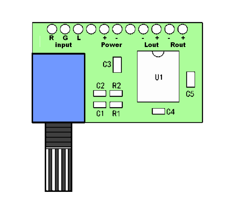
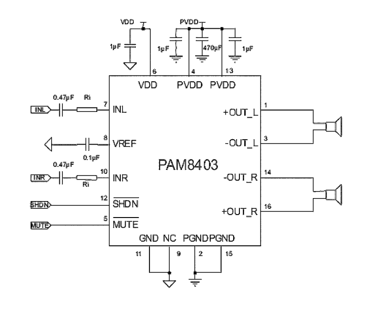
Encapsulated in a plastic case for SMD (is a SOP-16, as seen in figure), the PAM8403 allows to obtain, powered only at 5 volts, 2×3 watts on 4 ohm speakers (with 10% THD); its efficiency is 90% with 8-ohm load and about 85% at 4 ohms.

The chip contains a stereo preamplifier stage (two operational for each channel) and a double PWM modulator, each section composed by a comparator whose inputs compare the pre-amplified LF signal with a triangular wave generated by the internal oscillator. Each comparator has a differential output that drives a MOSFET final power ampli configured to bridge, the outputs of which are applied to a pair of floating pins (i.e. “raised” by ground mass); the final transistors do not require polarization because they are driven only by pulses produced by the comparator.
The internal circuitry is completed by the PAM8403, a logic circuit that allows both to switch off the device controlled by the /SHDN pin (the IC remains powered but absorbs very little because the power stage, the oscillator and the PWM modulator are off) and the outputs muting (controlled by the /MUTE pin, it works by triggering a decoder that reduces the input stages gain to attenuate signal).
Another advantage of using the PAM8403 is that since the power to be dissipated is definitely low, the integrated requires no heatsink and no metal plates under the body (for dissipation through PCB traces), uncomfortable to be welded without hot air equipment; This means that you can weld it safely to an ordinary printed circuit board with a common soldering iron. An advantage not just for those who practice electronics for pleasure and does not have specific equipment for SMD assembly, such as hot air station: one more reason why we chose it for an amplifier design for everyone.
Even if it should overheat, the PAM8403 has an internal thermal protection that prevents it reaching dangerous temperatures.
Circuit diagram
Well, after a brief discussion on the most important integrated circuit in our project, we see how the PAM8403 is used in our stereo amplifier: the configuration does not differ much from the application scheme recommended by the manufacturer and shown in figure. We find the L and R inputs coupled through a capacitor each, having a resistor in series; the capacitor separates the continuous component which biases the preamplifier input from the circuit input contacts, while the resistance determines the gain and limits the effect of the passband potentiometer cursor position change.
The one-port R/Cs placed in series to inputs are R1 / C1 for the 10 pin (input R) and R2 / C2 to 7 pin (Input L); between the circuit input contacts and the associated PAM8403 inputs there is a double potentiometer that adjusts the signal level applied to the chip and then the volume control. This component, named SWP1, has a single-pole switch actuated by the same knob that adjusts the volume and which is open when knob position is on extreme left (volume = 0). Since the open switch means that signal is connected to ground in our case, that means that bringing the volume to minimum turns off the whole amplifier, since the switch is in series with the positive power input (from +PWR pin supplies pins 6 (input stages) and 4, 13 (power stage).
The double potentiometer right pins are connected to audio circuit inputs named INL and INR (referring to input ground ING). The circuit is completed by the capacitors C4, C3 and C5. C4 is applied to the Vref pin for voltage filtering. Vref is generated internally by a regulator that supplies the voltage reference and bias to the input stages and to the PWM comparator. C3 and C5, respectively applied between the positive U1 power supply (PVDD) and the power ground (PGND) and between the positive power of the input stages (VDD) and relative ground (GND).
Note that in PAM8403 the masses are different to prevent that the voltage drop caused by the MOSFET power stage pulses (controlled by PWM modulator) and by traces and pins resistance, even if really limited could get in as an unwanted feedback on the input preamps, causing instability and noise.

To keep power lines separate it is necessary to design the printed circuit with different traces from the contacts PWR + and – for the two power supplies, filtering locally, i.e. close to the pins described above, the voltages through ceramic capacitors (electrolytic are not needed because the frequencies involved are high, and then a ceramic by a few hundred nanofarads is enough).
In our circuit we decided not to use the shutdown and mute functions, then respective pins (/SHDN and /MUTE) are not connected: the U1 internal pull-up resistors keep them in logic state high. These pins in theory can also be left open, in which case the respective functions are disabled in the same way that by connecting them to the positive power supply, as 5 and 12 are provided internally with a pull-up resistor each.
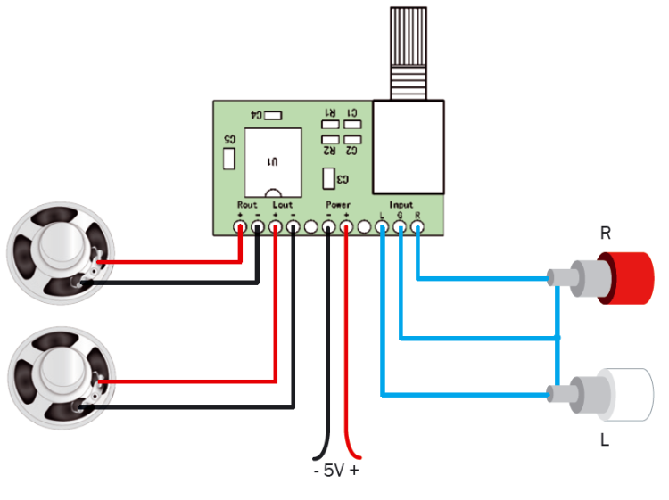
You can directly connect speakers to channel outputs (O-L, O+L for the left and O-R and O+R for the right): these outputs are bridged so we don’t need any de-coupling capacitor and in any case they work in an on / off duty cycle so they have zero potential when off; the only difference compared to the traditional output terminals (also called single-ended) is that they are not ground referenced, then the speakers are to be connected between the output pins and not to ground. By doing this, the output power becomes practically a quarter of that stated by the manufacturer.
Also, you must not short circuit the two speakers’ negative pins, because internally the two channels are separated (there is no common); if you short circuit them, you will damage the PAM8403.
From Openstore

Nice article.
How can I read back the volume level?