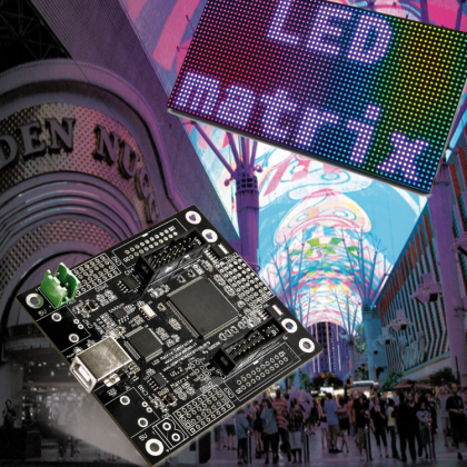
A dot matrix RGB LED graphic panel, managed by a FPGA-based controller board that may be separately used as a demoboard, so to evaluate the potential of the on-board Spartan 6. First installment.
In this post you will find the description of a graphic display that uses a modular solution based on dot matrix blocks (in which each dot is a RGB LED), that are driven – via a specific bus – by a very powerful control board, that is entirely programmable and capable of managing even very fast animations, thanks to the FPGA it is supplied with. Yes, the key factor is the Spartan-6 Field Programmable Gate Array by Xilinx, that is able to execute programs at very high speed, thanks to its parallel processing capability (multi-thread); the model that has been used in the project was chosen because it represents the most performing FPGA available on the market as a TQFP package, therefore it may still be soldered by means of the traditional tools. In order to create our modular display we are using a control board that will be described in the next pages; actually it is not limited to the said application, but it’s a generic and very powerful and versatile controller, whose advantages and the usage possibilities you will understand better in the next paragraphs and in the future articles. The displaying part is on the other hand composed by RGB LED dot matrices supplied with a shift-register; the whole will enable the management of a giant display with a 320×240 pixels resolution, each pixel is characterized by a 256-colour True Color definition at a 25 Hz refresh frequency, that is more than enough to show flicker-free moving pictures.
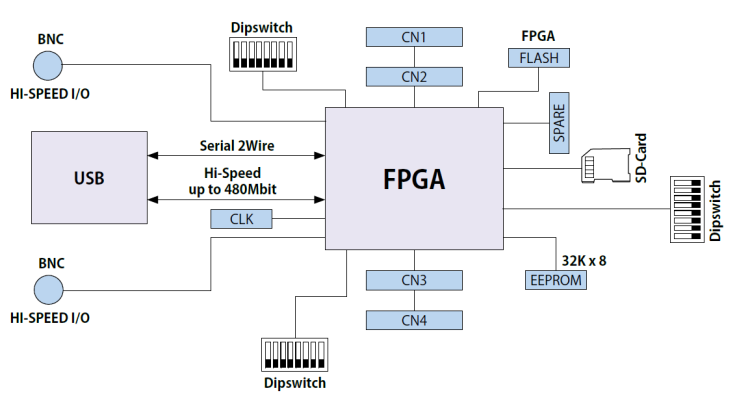
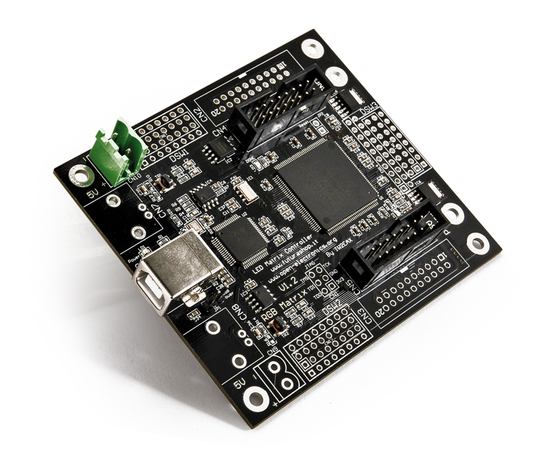
We will deal with the displays later on, since now it is the case to focus our attention on the controller board, that is a very powerful and versatile development board, based on a Spartan 6 FPGA XC6SL9; 62 out of its 102 I/Os are available for a generic usage, while the remaining ones have been assigned to dedicated functions such as the USB serials, the EEPROM memory, the SDcard, the Boot Flash, etc. Even though it is here used as a display controller, it may help you realize an infinity of applications.
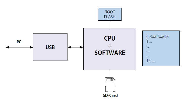
We coupled a Winbound Flash memory (signed as 25Q64FVSIG) to the FPGA, it will be the FPGA’s boot memory: a bootloader (that remarkably simplifies the programming) resides in it, and even 16 firmwares may be stored (thanks to the bootloader itself) by taking advantage of the possibility to store 16 slots for the bitstreams (the FPGA programs are thus called); out of the 16 slots, one (number 0) has been fixedly assigned to the bootloader, and the other 15 to the programs. The bitstream to be booted is chosen from the bootloader’s menu and directly from the terminal. The Flash memory is a 64 Mbit access serial one, that has been implemented thanks to dual/quad SPI configurable links.
In addition to the Flash memory, the FPGA may rely on a work memory to store the configuration data and more: that’s a traditional EEPROM, and still a serial access one.
The board has been designed so that the FPGA may execute the calculations at the request of a computer (via 480 Mbps USB) and also the programs written on SD-Card (that’s not a case it has a microSD slot); as for the USB connection, the innovative FT2232HL chip by FTDI has been used, it enables the obtaining, from a single USB 2.0 connection, of two virtual serial ports, that actually are (at a hardware level) a high speed serial one and a 8 bit parallel one; the two ports are a control and configuration (by means of the terminal) one and another one for streaming the data to be sent to the display.
The USB interface chip is fully programmable and the configurations have been written in a second EEPROM having serial access.
The programming may be directly carried out via USB, thanks to the preloaded bootloader; therefore both for the usage and the programs upload it is not needed to use the Xilinx JTAG cable, which means considerable money savings and a simplification in the board management.
An application is supplied, in addition to the bootloader, to immediately test the board for the purpose of managing the dot matrix RGB graphic LED panels (for a maximum of 4 32×32 panels).
The display management(via a PC) is carried out via the Jinx free software.
The board is also supplied with a serial input and a serial output with BNC, that are fully configurable, as an example in order to be used as input and output of a serial signal that is repeated on more boards connected in cascade.
They might also become signal inputs to be monitored, in future applications, but as for this application they work as explained above.
The hardware of the demoboard has been schematised in Fig. 1, and we suggest to look at it before proceeding to the circuit analysis.
Circuit Diagram
It is now the case to deepen our knowledge of the board, by analysing the circuit diagram and starting from the FPGA (signed as U1) that, given that the unit starts as an evaluation board, has all the I/Os extended towards the pads: some have been thought so to host connectors, other ones for mounting pin-strips or dip-switches; for each group of lines it is possible to mount (on the corresponding bus) one or more connectors, pin-strips, etc. that will prove to be in parallel.
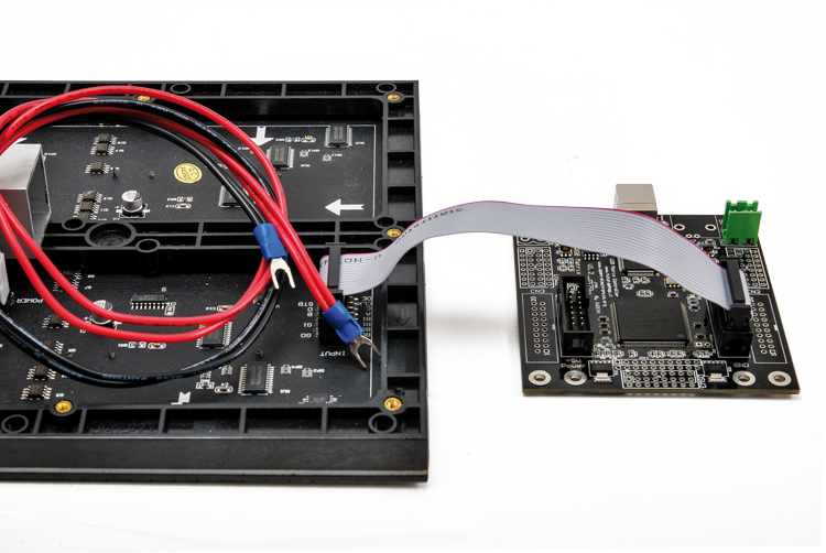
The connectors provided are 5: CN1, CN2, CN3, CN4, CN5 (the other ones are connected in parallel to these, and they essentially copy them); as for the giant matrix display we use the last two, that is to say CN4 and CN5, since one manages a group of 32×32 pixel, 64×32 pixel or 128×32 pixel modules (a single connection would not be able, for reasons of speed, to serve the whole panel).
We decided to extend all the I/Os towards the connectors and the pads where to mount both input devices and connectors, so to give you the possibility to use the board more comfortably, if you’ll decide to use it to develop applications that are different from the control of RGB LED matrices.
The arithmetic logic unit (ALU) and the FPGA’s logic devices that require it, will receive the clock from the IC1 quartz oscillator (Xpresso by Fox); the clock enters pin 84 of the Spartan 6.
The SD-Card reader’s data channels – respectively DAT0, DAT1, DAT2, CD/DAT3 – are connected to the IO_L52P_3 (6), IO_LIP_HSWAPEN_0 (144), IO_L36N_3 (29), IO_L37P_3 (27) lines; the SD-Card clock is connected to IO_L50P_3 (pin 10) while the CMD channel goes to pin 11 (IO_L49N-3). All these lines have been made accessible even from the TP1 (DAT2), TP2 (CD/DAT3), TP3 (CMD), TP4 (CLK), TP5 (DAT1) and TP6 (DAT6) test-points. Let’s make a digression here: in order to speed up the access to the Card – from which the FPGA firmware enables the execution of programs or, in the case of the matrix display, the download of data in order to rebuild the images in real time – we provided the usage of a faster mode, that is not the classic SPI to which Arduino and derivative products used us to, and that is used by the consumer microcontrollers; here we use the full-speed mode by separating the data from the commands (that instead, in the SPI and I²C buses travel on a single wire or two, in the case of the SPI having MISO and MOSI) and using as many as four bidirectional lines for the reading and writing of the data; they are DAT0, DAT1, DAT2, DAT3, and along these lines they travel in packets and are then recomposed at the appropriate moment. As for the commands, we use the CMD channel and all the communications on DAT0÷DAT3 and CMD are marked on the clock that FPGA sends to the homonymous line. And now we come to the USB interface, that deserves our attention since it has been created with a FTDI integrated circuit, whose name already gives an idea of its possibilities: FT2232HL (it’s a UART/FIFO dual USB); in fact, it behaves as a double FT232, since from a single USB 2.0 Full Speed connection having two wires (D+ and D-) it obtains two virtual serial ports, that (at a hardware level) actually are a high speed serial one and a 8-bit parallel one. The driver supplied by FTDI anyway enables the management from Windows, as for two virtual COMs, to the point that when we connect our board to the computer and we install the drivers, we see a pair of COMs open. To have two virtual ports on a single USB enables to use one for a task and the other one for something else, that is to say, to use one for loading the firmware and the other one for acquiring data. The serial port refers to the U2’s SER_TXD and SER_RXD lines; the parallel one is on the other hand located on the bus composed of USB_Data_0÷USB_Data_7. All of them, along with the USB_RXF, USB_TXE (it enables the transmission from inside of the board to the USB bus), USB_OE control signals, etc., enter the FPGA. From the circuit diagram it is possible to notice that the two virtual serials have been used in a different manner, one in fact uses the classic TX and RX in order to exchange data with the PC, on the other hand the other peripheral is used in parallel, so to have a data exchange with the FPGA at a much higher speed.
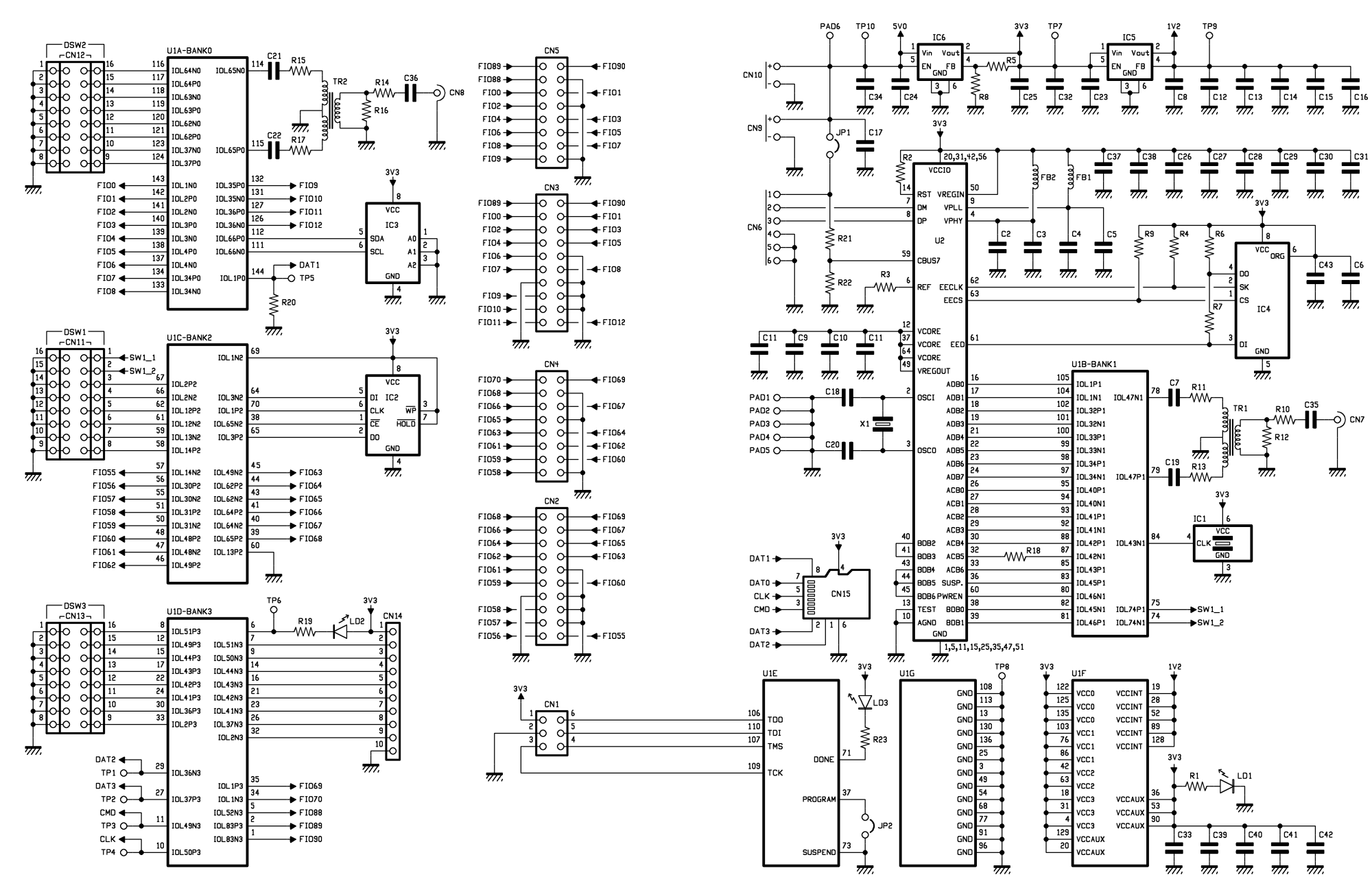
As with the FT232 (that we know well, since we used it in many projects), even the FT2232HL is programmable, however the configuration is saved in a Microchip 93LC46 external EEPROM, given that the integrated circuit does not have an internal EEPROM. The clock for the USB/serial converter has been obtained from a 12 MHz quartz, that is connected between the OSC0 and OSC1 pins, each one of them has a capacitor that ends to ground, so to harmonize the oscillator.
The FPGA boot memory (that is to say, the one that contains the firmware to be executed) is the W25Q64, a 64 Mbit one by Winbound, that is serially managed via a SPI that depends on the DI (input data coming from U1’s pin 64), DO (output data read, sent to the FPGA’s pin 65), CE (Chip Enable, managed by FPGA’s pin 38) and CLK (clock input as for the communication, supplied by FPGA’s pin 70) lines.
Moreover, the FPGA may rely on a non-volatile memory, that is the EEPROM 24LC512 (512 Kbit), that contains the characterization data and other settings of the program to be executed; the memory is a serial access one, via the I²C bus, that has been implemented by the EEPROM SCL (FPGA’s pin 111) and EEPROM SDA (FPGA’s pin 112) lines, that act as an output. The address on the bus chosen for the EEPROm is 0, given that all the three pins provided for the setting of the address’ last bits (A0, A1, A2) are to ground.
Until now we have seen the digital lines, but in the demoboard two connections for high speed signals have been provided, they may be accessed from the BNC connectors that are signed as CN7 and CN8; we need them if we want to send or receive data streams, that is to say, analog signals that have been sampled and that are available in the serial format, and also to create measurement tools such as frequency meters and pulse counters. The two sockets may be indifferently used as inputs or outputs, thanks to the great flexibility characterizing the FPGAs.
In the display control applications they are used as a feedthrough, in the sense that if we are creating a display having a great size and if in order to drive the RGB LED panels we need more boards, the one connected to the computer’s USB will receive and send the data to the FPGA, which has then to divide them in packets and to decide which ones to use in order to command the display part that is connected to it, and which ones to send to the BNC, that in this case acts as an output.
The board that – following the order – comes next, is connected in cascade by means of the other BNC and keeps the data concerning it for itself, while it repeats on the BNC output the unrelated data, that will have to reach the other boards.
The peculiarity of the lines on the BNC is that – differently from all the other I/Os – they are differential ones and are uncoupled on the demoboard by means of signal transformers (TR1 and TR2) with centre tapped secondary winding that convert the unbalanced signal (coming from the BNC) into a balanced (differential) one for the FPGA, but without altering its linearity.
Their processing will then occur by means of the FPGA blocks, that are selected by the application’s firmware, from time to time. Please notice that the “differential” expression concerns the internal side of the board and not the BNC: in fact, the inputs are unbalanced at the BNC (that is to say, they are connected to a contact with respect to ground) while from the FPGA side they are balanced, that is to say they refer to two I/Os. Each BNC is uncoupled by means of a capacitor in series to the signal’s wire, so that if devices having a DC polarisation are connected to the demoboard, the transformer does not act as load; moreover, a 75 ohm resistor is in series to each BNC, and it stabilizes the input impedance to such a value.
On the internal side, the transformer with centre tapped secondary winding (connected to ground) supplies two signals in phase opposition; each one of them, by means of R/C dipoles in series (so to uncouple and stabilise the impedance) it is connected to a pair of FPGA’s I/Os.
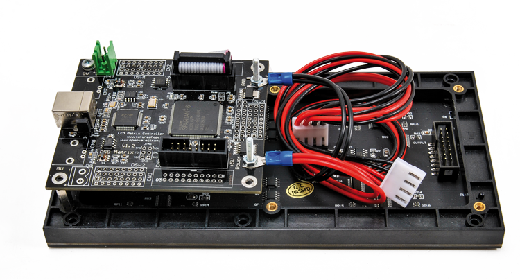
The whole demoboard may receive power from two distinct sources: the USB or a specific connector that is signed as CN9 (actually, there is also CN10, that is in parallel to it and is needed in order to bridge the power from a board to the other one if more than one is assembled) in the circuit diagram; in the case the power is drawn from the USB, the JP1 jumper must be closed, and it must be left open if – even if connecting the USB – we prefer to power from the connector, for reasons of absorption on the part of the demoboard.
It is not advisable to leave JP1 closed, if we power the board from CN9/CN10, since the two power lines would conflict and that could cause damage to the PC, were it turned off with the board being still powered.
Inside of the board there are two regulators of the TPS73831’s kind: the first one draws 3.3 stabilized volts from the 5V coming from the USB or that are anyway received from CN9, while the other one receives the stabilized 3.3V and draws the 1.2 V needed by FPGA’s calculation core. Each one of the power sources (3.3 and 1.2 V) is heavily filtered by a battery of ceramic capacitors arranged along the corresponding lines that go from the regulators’ outputs to the integrated circuits’ pins. The 5V line may be accessed from the TP10 test-point.
The project
Now that we know the hardware in detail, we may deal with the functioning of the demoboard inside of our project and with the specifications of the matrix visualizer, that will make us understand which ones are the problems inherent to its creation. Let’s start by saying that if our visualizer has be composed of a maximum of 48,000 pixels (that is the limit of the display control software that we used, Jinx), with a 4:3 aspect ratio (the one of a traditional television); since the study of Optics tells us that in order to view moving pictures that are flicker free, and without perceiving the frame, we need to compose at least 24 images per second, we will round it up to 25, therefore the refresh-rate (that is the update frequency of the frame) is equal to 25 Hz.
Under these conditions, the controller (that in our case is the FPGA) gets data produced at the frequency of:
f = 25Hz x 48.000 = 1.2 MHz
that is to say, as many Mbit/second.
But since we want to view colour images and for that purpose we drive panels composed of RGB LEDs (so to compose the colours with the combination of red, green and blue), such a frequency must be multiplied by 3 colours, which brings us to 3.6 MHz.
But that is not that simple, since in order to obtain all the colours, that is to say a True Color resolution, we have to combine the three colours, therefore for each LED of each subpixel we have to modulate the brightness, so to provide a hue; we will make it at 8 bits, since we want to obtain 256 hues for each of the primary colours, which will bring to 56x256x256=16,777,216 colours! But such a colour resolution carries the cost of multiplying the display refresh frequency by 8, since the FPGA must produce, for each subpixel and at the refresh speed of 25 Hz, as many as 8 bits in sequence; therefore the definitive working frequency, fd grows to:
fd = 3,6 x 8 = 28,8 MHz
that is to say, a data rate of 28.8 mbps on serial.
But it does not end here: in order to modulate the brightness of the LEDs, the data towards the display will have to travel at an even higher speed, since when carrying out the control we subdivide the lighting period for each one during the refresh interval, that amounts to 1/25 of a seconda (40 ms); more specifically, we opted for 256 brightness levels, corresponding to as many lighting periods of the LEDS; each one having a duration of 0.156 ms. That is why the engaged bandwidth (Bw) actually grows to:
Bw = 28,8×8 Mbps
corresponding to a 230,4 Mbps data-rate, that is fully supported by the hardware.
In order to modulate the brightness for each pixel, we therefore play on the duration of the bits concerning the lighting of each LED.
For this reason, in addition to the USB, the computer used for sending data to the board, the SD-Card possibly used for loading the program and the serials on BNC must be fast as well.
In the case the display is managed by a specific computer software (we chose Jinx, of which we will tell later) the USB port must guarantee a USB 2.0 Full-Speed data flow; the USB/serial converter we used satisfies such requirements, while if we had used a FT232RL we would have stopped to 3 Mbps as for the serials.
Once the data has been received from the FPGA, the last one starts to work, and it is a very complex and demanding one: as a first thing, the pieces of data are broken in two packets for each block having a 32 pixel height, since the LED matrix modules we chose are organized like this: they accept data in 1:16 multiplex, therefore it’s 16 LED lines at a time on a single data channel. For this reason, two distinct streams are needed for 32 LEDs. Therefore, the FPGA breaks the pieces of data and sends them on two lines for each display block, they are repeated on the CN4 and CN5 connectors; since – and we will see it soon – each matrix display has a shift-register as an interface element, the pieces of data are flanked by the strobe signals and by the clock. Each string that is related to a 32×32 module’s line is 4 byte long, each module is loaded with a strobe pulse. In summary, the FPGA commands 6 data lines for each 32×32 pixel display block: that’s two for each primary colour. In order to obtain a full display we therefore need four boards.
Please notice that the multiplex ratio significantly influences the panel’s overall brightness. This means that if in a certain fraction of a second the pieces of data as for 16 pixels are sent, each one will be lighted for 1/16 of the time, while if the pieces of data as for 8 pixels are sent, each one will be lighted for 1/8 of the time (that is, double the time).
And precisely the multiplex ratio and therefore the number of pixels managed by a single shift-register, concurs to determine the quality of the LED matrix panels and, in particular, it determines its brightness; it is then clear that the best results are obtained without multiplex, that is to say with a low ratio, but that means a much more substantial and expensive electronics, which is almost unattainable.
The panels we use in this project represent a middle way between costs and visibility (brightness), and we may consider this as a good compromise.
Since a demoboard is capable of driving a maximum of four 32×32 LED or four 16×32 LED matrices, in order to compose and drive a panel with more models like these, the firmware provides the repetition of the data stream concerning the contents to be proposed, by means of the BNC connectors; in practice, if from the PC the software sets a picture exceeding 32×32 pixels, the stream is repeated on the CN8 BNC, so to send it to the CN7 in the next board. The firmware is in fact designed so to repeat on one of the BNCs what enters in the other one, so to have the boards in cascade. Each one of them will then deal with the picture’s part within its competence, and will ignore the remaining pieces of data. The data streaming on the BNCs is carried out at 135 Mbit.
The displays
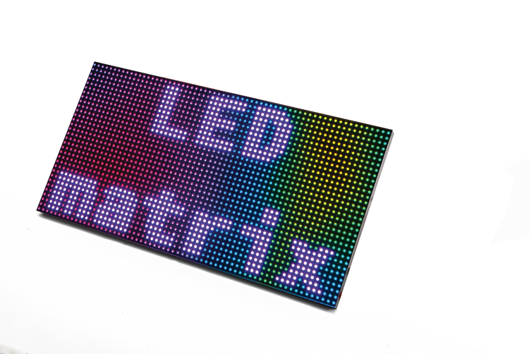
The visualizer may be composed by means of the coupling of more elementary 16×32 or 32×32 RGB LED matrix panels, each one of them is then driven by a CN4/CN5 connector of the demoboard; the panels are sold in our store have the RGBLEDPANEL3232 code. Independently from the matrix type, the connection is carried out by means of the CN4 and CN5 connectors: one drives two matrices for a maximum of 32×32 LED each and the second one drives the remaining ones. Each matrix of a group – that has an input connector and another one for the connection in cascade – is connected in series to the other one: therefore the first one is connected to the board and the second one to the connector repeating the first one.
Each panel (independently from how many LEDs form the matrix) has two IDC connectors, one for the data input and the other one for the output, enabling to connect more panels in cascade, so to form even bigger screens. The panel’s power source is a DC voltage one, having a value ranging from 3.3 to 5 V; the absorption is of about 2A for the 16×32 one, and of around 4 A as for the one with 32×32 LEDs.
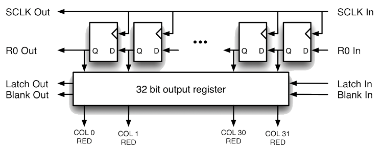
Let’s take a 32×32 LED module into account, it counts 1,024 RGB diodes, horizontally divided in two 32×16 bit halves; the upper half consists in 32 columns by 16 rows, and the same goes for the lower half. The display columns are driven by a set of drivers, and the display rows are driven by their own set of drivers.
In order to light a certain LED, it is needed to activate the drivers as for the row and the column at whose intersection it is found. In order to set the desired colour hue, every primary LED (red, green, blue) is individually driven on the corresponding free electrode, therefore as regards the rows a common terminal (commanded by the corresponding row driver) is found, while as for the columns there are three drivers for each RGB LED, that drive the independent terminal.

shows the panel’s internal organization.
Each panel contains six groups of column drivers; three for the upper half and as many for the lower one. Each driver has 32 outputs. The three drivers in the upper half drive the red, green and blue junctions of the 32 LED columns in the 0÷15 rows, while the three drivers in the lower half drive R, G and B of the rows going from 16 to 31. The column drivers are three shift-registers, one for each colour, and they serve a 32 bit block; a shift-register is ideally composed of a flip-flop cascade, that is supplied with an input whose bits are serially introduced, one by one, and each one is marked by a clock impulse. In this specific case, the register outputs are all connected to a latch, that is normally deactivated; it is activated by presenting on the outputs the pieces of data received as an input by the outputs of the (register) counters; in this way we may load all the bits corresponding to the columns in the shift-register, then “open” the latch and present them all together on the LED matrix by sending a strobe pulse, at the end of each string.
Also, the blank line operates on the latch, instantly switching off all the LEDs, inhibiting the outputs of the registers and therefore preventing the current to flow in the LEDs.
The inputs for each shift-register triad refer to Rx, Gx, Bx: R0, G0 and B0 are the inputs given for the upper part of the 32×32 block, and R1, G1, B1 are the ones for the lower part. The blank, strobe and clock (SCLK) lines are on the other hand common to the registers of the whole display.
The rows are directed by means of 4 address bits and a decoder. The 4 bit input used for the addressing is decoded and the two drivers corresponding to the set address are consequently activated.
When the A/3-0 addresses are at a logic 0, the rows from 0 to 16 are lit, while if the A/3-0 are at 1, the rows from 1 to 17 are lit. It goes on, following this outline from time to time, until the value becomes 15, as soon as the rows from 15 to 31 are activated.
In addition to the row and column logic, the display is provided with a blanking input, that is physically connected to the column driver. When the blanking signal is sent (that’s a logic 1) all the pixels are switched off and the display will appear black, that is to say, inactive.
In order to display a flicker-free picture, and without ghost images, all the signals described until now must be used with the appropriate timings.
Conclusions
In the next post we will deal with the FPGA software, the terminal we created for interfacing it, and the Jinx application: the heart of such a powerful machine like our FPGA-based demoboard.
From openstore

[…] A FPGA controlled RGB LED MATRIX for Incredible Effects – [Link] […]
[…] A dot matrix RGB LED graphic panel, managed by a FPGA-based controller board that may be separately used as a demoboard, so to evaluate the potential of the on-board Spartan 6. First installment. In this post you will find the description of a graphic display that uses a modular solution based on dot matrix blocks (in which each dot is a RGB LED), that are driven – via a specific bus – by a very powerful control board, that is entirely programmable and capable of managing even very fast animations, thanks to the FPGA it is supplied with. Yes, the key factor is the Spartan-6 Field Programmable Gate Array by Xilinx, that is able to execute programs at very high speed, thanks to its parallel processing capability (multi-thread); the model that has been used in the project was chosen because it represents the most performing FPGA available on the market as a TQFP package, therefore it may still be soldered by means of the traditional tools. In order to create […] – Read full story at Hacker News […]
[…] A FPGA controlled RGB LED MATRIX for Incredible Effects – the HardwarePosted 2 weeks ago […]
[…] A FPGA controlled RGB LED MATRIX for Incredible Effects – the Hardware – Open Electronics – pěkné – Spartan6, USB do PC, 16×32, 32×32 a 64×32 px […]
Great Post, I wonder if I can also use a Logi-Bone and Beaglebone for the project.
[…] applications we proposed in the past concern 32×32, 64×32 or 128×32 pixel (LED) matrices: and they are based on a free […]