A new Arduino-like board appears on the horizon ready to “devour” the competitors: not surprisingly, it was called Shark! Let’s see its features. First episode.
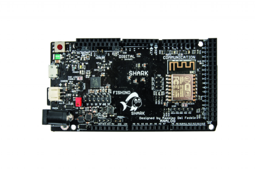
A shark appears in the Fishino sea, whose sharp teeth are its leading characteristic: they allow it to “bite” the applications. Shark, as we called this new board, belongs to the 32-bit series based on Microchip’s PIC32MX microcontrollers. Like the other 32-bit Fishino, it maintains good compatibility with the Arduino system, offering significantly higher performance and memory capacity. Shark was born out of the necessity to, after the Fishino 32 that was compatible with Fishino UNO and packed with an excellent audio codec and Fishino Piranha that was compatible with Arduino MKR1000 and packed with additional functionalities, make a 32-bit board with I/O pin functionality for complex applications that require greater hardware connectivity. Fishino Shark provides 32-bit performance and peripherals in the format of an Arduino / Fishino MEGA. Thanks to a specific bootloader, a long press of the reset button is enough to update the firmware of the WiFi module and the board will automatically set itself in update mode from the USB connector.
If you’re worried about the programming of this board, have no fear; thanks to the versatility of the current Arduino IDE, the work of Chipkit’s team that we have partially exploited (with several changes) and the software libraries we wrote and/or adapted, the programming is performed like on a common Arduino UNO, i.e. through the IDE, in which you have to activate the development tools for the PIC and you’re done!
For the additional components, we have set up a series of libraries, some of which are in ongoing development. We recommend that you visit the website periodically.
WIRING DIAGRAM
The scheme is largely similar to Fishino32, but right now we’re going to use a micro with more I / O, almost identical to that of Fishino32. We have 100-pin here while in the “small” model is 64-pin.
The same microcontroller is available with clock frequencies ranging from 80 MHz to 120 MHz. While on the Fishino32 we were able to use it at 120 MHz, on the Fishino Shark we have foreseen the possibility to select the speed between 5 and 105 MHz.
The wiring scheme is very similar to Fishino32. Let’s analyze it and see the differences.

POWER SUPPLY CONTROL STAGE
This block is much more complex than previous models, for the following reasons:
- the need to function both as a host and as a USB device;
- triple power supply;
- the possibility of software shutdown of the entire power supply stage;
- the possibility of activating the standby controller power supply only.
Let’s start from the control section of the USB power supply. It must be able to supply voltage to Shark through the USB connector is connected as a device and adequate power supply to a device possibly connected to the board when the latter operates in USB host mode. For the switching, we can use the pin attached to the USBID line, connected both to the USB connector and the controller port.
Don’t forget that the microUSB cables are set to have at one end the pin corresponding to the USBID connected to ground (type A) and to the other the same unlocked pin (type B); the device to which the type A end is connected to will take the initial host role and at the same time will supply energy to the other device, connected to the type B end (which will initially take the role of device). The expression “initial roles” is a must, because, in an OTG connection, the two USB devices can change roles; the specification only guarantees that the line will always be powered by the device connected to the A end.
Let’s go back to our scheme; we can see that the USBID line is connected to a high-value resistance (R2, 100 KOhm) to ground, the purpose of which is not to leave the line floating in the event of power failure, and a resistance (R4) of much lower value (10 KOhm) connected between the sources of the MOSFETs Q4 and Q5. On these, thanks to the diodes inside the MOSFETs, there is always a positive voltage (5V minus the direct fall on the diodes) coming either from the USB socket or from the 5V power supply of the Fishino board. We, therefore, have the certainty that the R4 is connected to + 5V in any operating condition. If the USBID line is disconnected from ground (type B connection) this positive voltage, through R4, conducts the N-channel MOSFET Q3, which in turn leads Q1 to conduction; at the same time, through R4 again, the two MOSFET Q4 and Q5 are placed in interdiction and connected in anti-series, do not allow the passage of power from the 5V Fishino to the USB connector.
Summing up, it has a floating USBID, so when we insert a type B connector, Fishino does not supply power to the USB connector which, on the other hand, feeds Fishino through the Q1 MOSFET. So we get the first part of the desired purpose: a type B Fishino connector that draws power from the USB line by acting like a real device. If we insert a type A connector instead, the USBID line is placed to ground, which leads to Q4 and Q5 conduction and at the same time, always through Q3, in Q1 interdiction; the power then flows from Fishino to the USB connector and does not fall “from the service port”, being Q1 interdicted.
Note that in the second case (connection type A) in order to supply the 5V to the USB port, Fishino must be powered by the battery or the VIN plug, as we’ll see later.
Continuing the analysis, we can see the series of diodes D1 + D4 and D2 + D3: the first two are for small currents, while the latter is of power. We can also see the MOSFET Q2, which is fed by the battery. Diodes D2 and D3, together with the MOSFET Q1, constitute a power OR gate that flows into the VOR line of the scheme. For diodes, the operation is the following: the higher voltage between VIN and VUSB is transmitted on VOR, while the other, due to the interdiction of the corresponding diode, inversely polarized, is isolated.
One might wonder why we didn’t simply insert a power diode like for the other two on the battery line, since it would have simplified the circuit, creating a power OR port with three diodes. It’s achievable, but there’s still the problem of the voltage drop on diodes: with high voltages it’s practically irrelevant, but it leads to considerable losses on a reduced voltage : we can say that a voltage drop of 0.5V on 10V corresponds to 5%, while the same drop to 3.6V affects about 14%, which is reflected in the current absorption as we will see below, and just where it would need more efficiency, or in battery power.
The MOSFET Q2 doesn’t have this problem. Unlike the diode, it doesn’t have a minimum voltage drop but a conduction resistance, very low in the model used; on the other hand, a MOSFET does not have the advantage of the diode to conduct only when it is needed, so a system is required to send it into operation or ban it. To do this we’re going to use the two diodes for small currents D1 and D4; the operation is as follows:
- if there’s no power supply neither on VIN nor through VUSB, the resistance R3 brings on earth the Q1 gate which then conducts and makes possible the transition of the battery’s voltage toward VOR;
- instead, if there is one of the two (VIN, VUSB or both), one of the diodes D1 and D4 conduct, positively polarizing Q2 which on interdiction, disconnecting the battery.
In short, if we have an external power supply, which comes from the VIN plug or USB connector, the battery is disconnected; if instead, the external power supply is missing, the battery starts working.
It can be noted that the line on which the diodes D1 and D4 converge has a name, BATOFF: this signal, which is at a high level if an external power supply is present, will also be used in another section of the circuit.
Let’s move on to the circuit section belonging to the MOSFETs Q6 and Q7; these are used to disconnect the + 3V3 line, i.e the main line at + 3.3V, from the + 3V3Core line, destined to power the controller only. What are they used for? Simply to avoid that a power intended only for the microcontroller, activated when all the rest is turned off in order to keep the internal RTC active and other minimum functionalities, will flow into the circuits that we intend to keep off. Normally, if the voltage is present on + 3.3V, this flows through the internal diode to Q6, and also through the Q6 itself if it is conducting, on the controller power supply + 3V3Core; this is normal functioning. Instead, if we remove the power supply on + 3.3V, and at the same time bring the OFF line to low, through Q7 we bring the Q6 to interdiction and therefore prevent the + 3V3Core from going to power the rest of the board. The OFF line is controlled by the controller, as we will see later during the programmed shutdown.

You can then notice the maintenance lithium battery G1 and the diode D6, which are used to supply voltage to the controller when it lacks any another thing that can power it. Be careful: if we completely remove the power supply to Fishino, this battery ends up powering the entire board, unless you “take action” through the software by bringing the OFF line to the lowest level. Unlike 8-bit boards, where the battery was only used for the maintenance voltage of the RTC and handled automatically, here it’s necessary to support the software, otherwise, the battery would be discharged in a few minutes.
We, therefore, advise not to use it, and leave the retention to the rechargeable LiPo battery, unless you know how to manage the energy saving of the board via software.
Finally, the PWRGOOD line, connected to a divider with the mass; this provides a positive signal to an I / O of the controller that indicates the presence of an adequate power supply on the board and can be used, in fact, to manage the lack of this and the standby functions.
As mentioned above, this is rather complex management, for which a special software library has been prepared, still under development, to manage the standby modes.
We advise you to look at the code and examples of the FishinoLowPower library to understand how it works!
The last part of the section in question is that which revolves around the linear regulator U1, a simple low current regulator (max 100 mA approx.) And very low consumption, designed to supply the holding voltage to the controller through the external LiPo battery.
This has the same effect as the G1 lithium battery, with the undoubted advantage of using a rechargeable battery able to provide extremely long life even in the presence of not negligible consumption.
This section can be deactivated by cutting the BCK jumper, normally connected. Even here (even if in a less pressing way) the energy saving talks made before: if we switch off the board via software, the controller will take power from the LiPo battery, which will then tend to discharge; moreover, if we exceeded the absorption 100 mA, the small linear regulator would “sit”, cancelling its output voltage. It is therefore always the task of the software to make sure that the controller is placed in standby or in any of the low power modes available.
SWITCHING POWER STAGE
This stage belongs to the integrated U2 (SX1308), a step-up asynchronous converter used we’re using here in SEPIC mode, able to provide a 5V output with input voltages ranging from about 3 to 20V, and to the integrated U3, which is a synchronous step-down converter, used to derive the 3.3 V supply for most of the circuit.
Both of these stages have already been extensively described for the Fishino Mega and Guppy boards and, as regards the operation of the SEPIC, in the Torpedo board. The only differences consist in the presence of the ON jumper, which allows the insertion of a power-off switchable to remove the power supply to the whole board (except for the maintenance one enabled, as explained in the previous paragraph), and the line OFF, already seen before, able to switch off, if carried to ground, the switching converter.
This line is under the direct control of the processor through an I / O and therefore allows both the complete shutdown of the board via software and the isolation of the power supply section of the controller alone from the rest of the circuit.
In summary, by placing the line OFF to ground, all the power supply to the board is removed; obviously this line must be kept grounded by the controller, which must, therefore, remain operative through one of the two maintenance sources (LiPo or lithium battery); in the absence of these, bringing the line OFF to ground we will get only a reset of the board and the consequent restart of the whole.
BATTERY CHARGER STAGE
This stage also belongs to the integrated MCP73831, a complete integrated charge controller for single-cell LiPo. Here the only noteworthy element is the MOSFET Q8, an N channel used to enable or not the battery charge function.
Like we said in the description of the first stage (power supply control), the BATOFF line is at a high level when an external power supply is present; in this case the MOSFET Q8 goes into conduction, bringing to ground the resistance R15 (and eventually the R16 if we have selected the charge at 500 mA), thus activating the charge. In the absence of external voltages (battery power supply) the BATOFF line goes to a low level by deactivating the charge.
To complete the description let’s see the resistors R17 and R18, which constitute a voltage divider able to provide half the voltage of the LiPo battery, measurable through a line of the controller to be able to signal the state of charge of the same. We used a divider because the voltage of the LiPo battery, at full charge, exceeds 3.3 V tolerated by the analogue inputs of the microcontroller; this must, therefore, be taken into account.
MICROCONTROLLER SECTION
Finally, we can talk about PIC32MX470F512L, a 32-bit high-performance capable micro-controller, which has quite small consumptions and a large number of devices.
Firstly, we can see that it has two quartz, one running at 20MHz and another one running at 32,768 KHz. But, why two quartz? Because the first one provides the main clock through an internal PLL which multiplies it up till 105 MHz; It isn’t a low-power circuit, so you should avoid it in case of energy saving.
The quartz running at 32.768 Hz is used exclusively for the real-time-clock (RTC) inside the PIC, which is a circuit studied in order to get a really low absorption and which can be kept in operation even in a stand-by condition.
Talking about the first quartz, by accepting a lower accuracy on the frequency, this one could have been removed because the PIC integrates an RC oscillator quite precise, but which has two limits:
- doesn’t provide the quartz accuracy
- it isn’t able to bring the PIC on its peak frequency of 105MHz, because of the PLL limits which limit it on 96MHz.
The first point matters only if we use the board for accurate measures of a short period of time: for example, as a frequency counter or as a period meter; for a long period of time, we can use the other quartz.
The second point is mandatory if we want to exploit the controller at its peak performance.
As you can see, there are the OFF lines from the micro, which allows it to switch off the main power, PWRGOOD, which allows the state control of the latter, and MBAT which allows to measure the battery’s voltage.
In this board, since the externally accessible I/Os are many, we had to multiplex some functions on single pins: PWRGOOD, for example, is overlaid with the analogue input AD13; if we use this one, the PWRGOOD’s functions are not available and conversely.

RESET AND LED STAGE
This stage is quite interesting because it allows us to use a single reset button for various functions, in combination with a special bootloader on the controller.
We immediately notice three lines that refer to the reset stage:
- MCLR
- REMOTERESET
- LONGRESET
The MCLR line is the actual reset and if you bring it to ground the microcontroller is restarted. This can be done either by pressing the reset button (through the capacitor C22 which transfers a short logic zero pulses to the MCLR line) or by bringing to ground the REMOTERESET line, coming from the WiFi module and thus allowing this to reset the micro.
The LONGRESET line, on the other hand, is found to be grounded for as long as the reset button is kept pressed, thus allowing the bootloader to know our intentions.
In summary:
- a short press of the reset button (less than 2 seconds) or a logic zero on the REMOTERESET line restarts the card;
- by keeping the reset button pressed for a period of time between 2 and 4 seconds, the bootloader is started (highlighted by the flashing of the orange LED), thus putting the board in sketch loading mode;
- keeping the button pressed for more than 4 seconds starts the procedure to upgrade the WiFi module firmware, which is highlighted by the blue LED flashing.
However, once you have entered the two bootloader modes, simply restart the board and run the preloaded sketch by briefly pressing the reset button again.
Even here, due to the lack of pins, we had to share the LONGRESET line with an analogue I / O (the AD14); no problem, in this case, since if you press reset the input is not needed!
We have assigned two LEDs to the microcontroller (driven through the MOSFETs Q10 and Q11 to not overload the PIC I / O), multiplexed with the serial port 2, usable for any task (indicated on the board as RX / PRG and TX, respectively); using serial port 2, the LEDs will pulse in analogy with the input / output data. If we don’t use serial 2, we can manage LEDs via software.
The microcontroller is also connected to the usual LED connected to port 13 that is used in the tests of the board (BLINK program), through the Q9 mosfet to not load the output D13. Unlike the Fishino32, the D13 output is a normal I / O and does NOT have the additional clock functionality for the SPI interface, which is, like the Arduino / Fishino MEGA, on other pins.
WIFI STAGE
Even this stage has already been described in the previous boards, but here we find a rather substantial difference, so we’ll review it in detail.
The module always uses a firmware we have made, able to communicate at high speed through the SPI port and not on the serial port like in systems using the ESP8266; the difference in performance, as already noted, is remarkable.
On this board, on the other hand, we no longer see the ESPCONN connector to which we were accustomed to the previous 8-bit boards and to which some I / O and control pins of the exploited module were in charge, both to program it and, for some of them, as additional I / O.
Why this choice? Simply because in the Fishino Shark we have already freed up some of the I/Os that were used to communicate with the module and the SD board, which were 4, 7 and 10; we have also separated the I²C port from the two analogue inputs A4 and A5, thus obtaining 3 digital ports and two additional analogue ports available. Not only that, but two ports on the ICSP connector are also usable as additional digital ports (we will talk in detail describing the software), so we preferred to exploit the connections with the ESP module in another way.
Almost all the ESP lines (except for the analogue input) are now under control of the main processor, which allows us to carry out the following operations directly from the software, without committing any I / O:
- reset the module from software;
- switch off the module from software (which previously required the use of a Fishino I / O);
- load the firmware on the module without having to make strange connections or load particular sketches;
- redirect the serial output of the module on the USB serial port or on any other serial, both software and hardware, available on the Fishino.
But why “almost” all the lines? Here too, to save an I / O on the controller, we avoided connecting the RESET line of the ESP8266; the same functionality can be easily obtained through the ESP_CHPD line, which also serves to send the module in low-power mode.
Our software libraries already take this into account.
For the rest, almost nothing is different compared to the previous boards: the communication takes place through the SPI port, which also belongs to the SD-card and the digital pins D50, D51 and D53 on the large connector at the bottom of the board.
Since the used PIC has two built-in SPI interfaces, one wonders why one of these was not dedicated to the included modules (WiFi and SD) thus releasing the I / O D50, D51 and D53 completely; this was done because the second SPI interface is dedicated, in I²S mode, to the audio codec that is working full time on it.
At first we had chosen that road, to realize only later that it was impossible, for example, to play an audio file read from SD-card, since during playback the interface was totally committed with the codec with no possibility to access the SD.
It must be said that on the boards in Arduino MEGA format the three I / O above are dedicated to the SPI port, and if necessary we have the two I / O available on the ICSP port we were talking about earlier, and eventually all analog I / O which are however also usable in digital.
MICROSD INTERFACE STAGE
This stage is absolutely identical to that of the boards already seen; it uses the SPI interface, such as the WiFi module, while an internal I / O is also used for the selection of the card, thus leaving the I / O D4 free which was previously necessary for this purpose.
The only major difference compared to the previous boards is the absence of the stages of conversion levels (from 5 Volt to 3.3 V) as the PIC uses 3.3 volts as power, thus making it possible (and faster!) a direct connection. The only detail to keep in mind in the execution of existing sketches is that the board selection pin (CS) is no longer the 4 (or 10 in some versions of Arduino) but an internal pin called SDCS; it is, therefore, sufficient to replace all the references to the I / O 4 with the SDCS I / O (written just like that, since it can physically change from card to card).
AUDIO CODEC STAGE
And here we are at the juicy news in the Fishino32, the audio codec!
This is based on a chip, the ALC5631Q, used in many consumer products (tablets, audio players, etc.) and therefore equipped with remarkable performance while retaining a more than acceptable price.
The codec has the following characteristics:
- 24-bit stereo DAC (DAC) converter with a signal to noise ratio of 100 dbA and total distortion at -90 db;
- 24-bit stereo A / D converter (ADC) with a signal to noise ratio of 93 dbA and total distortion at -88 dB;
- a Class D stereo amplifier capable of delivering 650 mW per channel if powered at 3.3V on an impedance of 8 ohms and up to 2.8 W per channel if powered (as in our case) at 5 volts, on an impedance of 4 ohms;
- a stereo headphone amplifier, capable of delivering 45 mW of 16 ohms, which unfortunately will not be used in our card for reasons of space;
- 3 differential analogue inputs or a stereo analogue input (we use the latter);
- 2 pre-amplified analogue microphone inputs, both in differential mode (not used) or in single-ended mode;
- an input for a digital stereo microphone (this too, not used on our card for reasons of space);
- an analogue line output, to which it is possible to connect an external amplifier;
- a complete power management system that allows switching off the individual components of the codec if not used;
- a 6-band digital audio equalizer;
- pseudo-stereo and spatial stereo effects;
- circuits for removing the on / off noise in the loudspeakers;
- automatic management of levels (ALC) both in reproduction and in recording;
- High-speed I²S standard interface (24 bit / 8 to 192 KHz on the playback DAC and 24 bit / 8 to 96 KHz on the recording ADC).
As you can see, a series of impressive features, which will allow you to create, without any additional hardware that is not a speaker or a microphone, many projects involving digital audio. Between these:
- audio player (wav and Mp3);
- audio recorder;
- vocal recognition;
- musical synthesis;
- speech synthesis.
As you will see later, we have already implemented a player for .wav, .mp3 and .ogg / .ogb files; for the registration, we have available a library able to create .wav files. There is also an MP3 encoder, but its performance is decidedly inadequate and was included only for curiosity and to be able to do some tests; MP3 compression is in fact too expensive to be carried out in real time by our very powerful controller.
As already mentioned when we were talking about the WiFi module, the codec uses a dedicated SPI interface, used in I²S mode, for the management of which we wrote a special software library.
The codec also needs an I²C port (not necessarily dedicated only to him, and in fact, we have used the Fishino standard I²C port) to control all the various functions available.
We have created a special library that can control the operation of the codec; through this, you can, for example, decide whether to record or play, change the audio volume, adjust the equalizer, set the ALC, and so on.
As you can imagine, the controls are very numerous, so the library will be extended as the need arises.
On the wiring diagram of the section there is very little to add: as you can see, in addition to the codec we have some decoupling capacitors on power supplies and I / O, a capacitor for an internal converter designed to increase the voltage for the headphone amplifier ( C38) and a pair of resistors for the bias voltage (polarization) of the microphones. Nothing else!
Let’s go back for a moment on the I²S interface: it is an interface based on the SPI, expressly provided for the transmission of high-speed stereo audio streams; unlike the SPI and due to the fact that the signals passing through it must be in real time, it is practically impossible to use it simultaneously on several devices. The interface uses the usual SDI (MISO), SDO (MOSI) and SCK (clock) data pins, while the selection pin is used differently to select the audio channel between the two transmitted; there is also an additional clock line, used as a reference.
So we have, naming the pins from the master side, that is, from the point of view of the controller:
- MISO or SDI -> ADCDAT, ie data input from the A / D converter to the controller;
- MOSI or SDO -> DACDAT, or data output from the D / A converter to the PIC;
- SCK -> BLCK, which is the clock for the individual bits transmitted;
- SS -> LRCK, or the clock to differentiate left and right channel;
- MCLK -> reference clock, usually 4 times the SCK.
Also here we had to “multiplex” the codec I / O with as many I / O available on the external port at the bottom of the controller, and precisely the I / Os from 45 to 49.
By using the audio these I / O will therefore not be available for your applications; on the other hand, not using the codec we will have those free I / O and, above all, can be used as an additional SPI interface (called SPI0 by software) totally independent of the standard SPI.
Signals transiting from/to the codec are visible in Fig. 1.
In this image, the reference clock (MCLK) is missing, which is still a fixed clock of a quadruple frequency with respect to the BLCK.
We leave the description of the codec for the moment, which we will resume when we will deal with the software libraries.
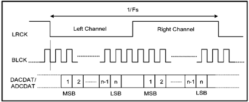
Fig. 1.
HEADERS
In this section we can see all the connectors that carry the signals to the outside of the board, then the side headers to standard Arduino, the double one at the bottom of the board, the ISP connector (which on Fishino Shark is not used to program the card, but inserted for compatibility with the existing shields), the ICSP (In Circuit Serial Programming) connector used to program the board without going through the bootloader (for example to program the bootloader itself), and on which two digital I / O are available additional, and the USB connector.
As mentioned by listing the characteristics of the board, the PIC used in the Shark has many, but not all, 5V tolerant pins, that is able to accept 5V input.
Where it has been possible, we have used those pins to take them out as digital I / O; unfortunately, in some cases, this hasn’t been possible and we have therefore inserted input protection by means of resistors and diodes. The protection consists of a 680ohm resistor in series at the input and a diode able to discharge the excess voltage on the 3.3-volt line, thus limiting the input voltage at that value.
On analogue pins, which are not 5V tolerant (just because of the internal circuitry inside the controller) we have inserted only the series resistance to limit a possible overcurrent in case you enter by mistake the values above 3.3 volts.
Be careful, this doesn’t mean you can insert 5 volts on that connector! The resistors offer a minimum degree of protection, which should protect the controller for short periods if the 5 volts are inserted by mistake, but they don’t have to be taken into account and use them permanently with those voltage values!
The integrated device has in fact protection diodes inside it, which act as replacements for those we put externally in the protected digital pins; these diodes, however, are able to absorb a very limited current and for short periods of time, so you absolutely must not be taken into account.
In the header section we also find a connector called REFSEL, which is used to select the voltage that will be connected to the VREF pin; in fact, it is possible to get the 5V, in case you use “normal” shields working at that voltage, or the 3.3V intended for low voltage shield like those used in the Arduino DUE.
CONCLUSIONS
This first episode where we introduced the peculiarities of our Fishino Shark board ends here, describing its hardware and operation. In the next episode, we’ll explain how to manage it from the IDE of Arduino and we’ll propose a first test sketch to see its potential.
From openstore
Fishino SHARK
Read the second part of the article —>

[…] Fishino Shark: arduino like board with 32-bit, WiFi, audio codec, sd card, battery charger … a…Posted 4 days ago […]