It is always convenient to dispose of an easily adaptable module that can play musical tracks: it allows to easily implement vocal syntheses to insert within a promobox, or to place items in the shop windows or in well trafficked areas, or close to automatic doors or to turnstiles, or to other automated terminals for various purposes. If the module is then capable to play tracks of a certain duration, and if it supports MP3 files (that have become the standard for various devices such as portable audio players, by now), we have hit the mark.
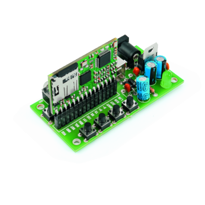
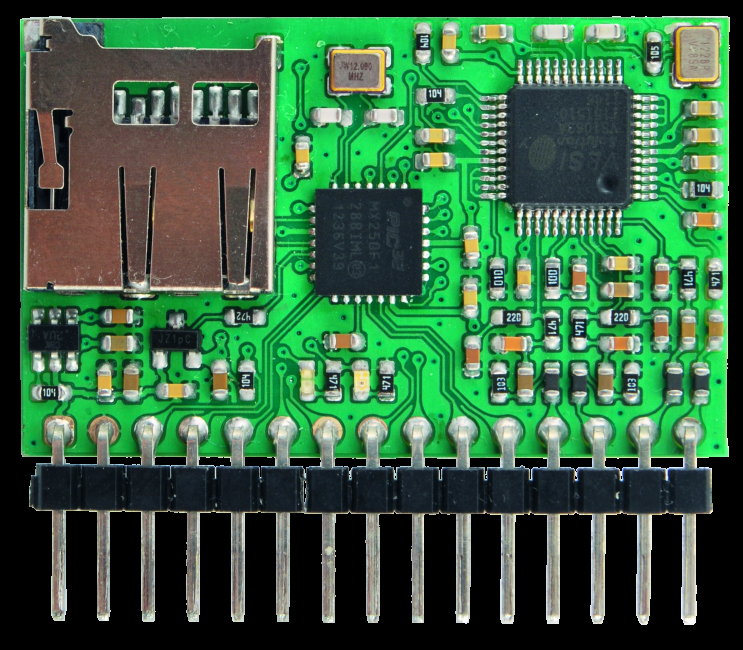
In this post we focused on the creation of a new electronic device, integrating both a player and an audio recorder inside. The supported algorithms for coding and decoding are: the now ubiquitous MP3 format and his direct competitor (and a royalty-free one), Ogg Vorbis. Everything has been thought so that each component needed for the operations is housed on a printed circuit having a limited size of about 25 x 40 mm.
This last one is supplied with a 15 pins angle header (Break Away Header), with 2,54 standard pin spacing, making it suitable for a vertical insertion in a breadboard, or for a combined usage with another printed circuit. The connector allows insertion and removal, as opposed to a dual female header, or to the permanent cabling in the case you prefer to weld the device to the hosting project.
The circuit supplies a microSD Push-Pull slot inside, operating as mass memory, and dedicated to the archiving of the recorded audio fluxes or as a support to the playback of musical tracks. Moreover, the circuit has all the components needed for the operations inside, thus it is enough to give a power supply tension and to select the interaction mode so that, in a short time, it is possible to hear your favourite track or to start a short or long term recording.
Circuit Diagram
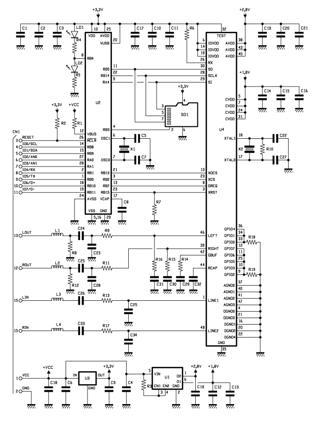
The MP3/Ogg Vorbis player and recorder is given life by the U2 (PIC32MX270F256B) component: this is a new microcontroller of the Microchip firm, a direct evolution of the PIC32MX250F128B microcontroller, and it allows pin-to-pin compatibility.
Both devices are supplied with a 32 bit RISC CPU, capable of operating with a 40 MHz clock frequency (50 MHz if the temperature interval is between -40° C and +85° C), reaching ideal conditions at about 80 DMIPS. Moreover, both devices are supplied with some communication bus standard hardware implementations: those are useful for our project. Among these, we remember: the Serial Peripheral Interface (SPI), used to access the microSD; the Inter Integrated Circuit (I²C), needed to interact with the exterior; and a Universal Serial Bus (USB) Client Full Speed peripheral.

The two microcontrollers differ for the quantity of available memory: the first one is supplied with a 128 Kb program memory and 32 Kb RAM, vice versa the PIC32MX270F256B has been designed to support two times the values for both the program memory and the RAM. Given the conservative pin-to-pin policy, both devices can be used on our circuit, but to obtain all the software functionalities, and to create without limitations it will be needed to choose the most powerful microcontroller.
Let’s continue the description of the printed circuit. The second most important component is the U4 (VS1063): this is a MP3 slave processor, produced by VLSI Solution, and even this component appears strictly as an evolution of his younger brother, VS1053. The main differences stay in the capacity to record in MP3 format, in addition to Ogg Vorbis. Moreover, the Ogg Vorbis format does not need the dedicated plugin upload at the moment of encoding: this makes the usage of the new device much more flexible.
As regards the power supply section, the circuit is provided with as many as 3 Low-dropout regulator (LDO) regulators. These last ones are there as two components: U1 and U3. Respectively, U1 (AP7312) hosts 2 LDOs in a very small (SOT236) package. In this particular model we used, these 2 LDOs give two stable tensions, respectively at 1,8 V and 2,8 V, with a maximum current of 150 mA, and they are used for the correct operation of the DSP section and of the VS1063 analog section. On the other hand, the U3 (AP7333) is a single LDO with 3,3 V output and a maximum current of 300 mA, and is used to supply power to the main microcontroller and to the microSD.
As regards the generation of the clock signals, the circuit has been provided with 2 quartz oscillators, respectively the X1 (20 MHz), for the purpose of supplying the 50 MHz needed for the proper operation of the software, by means of a Phase-locked loop (PLL) internal to U2; and X2 (12,288 MHz), needed for the operation of U2.
Finally, the circuit is filled with fitting combinations of discrete components, that allow to filter and attenuate the effects coming from the digital signals passing on the board, and to conveniently adapt the signals, according to the specifications of Line-In or Line-Out, as indicated in the analog section.
The Demo

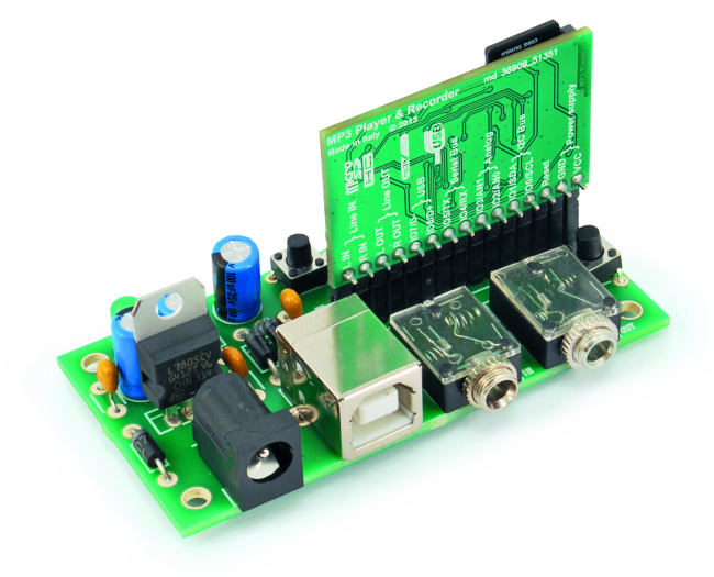
To allow the experimental usage of the reproducer, without the need to create sophisticated electronic circuits, we have produced the demo circuit. This demoboard shows how to easily interact with the reproducer, by supplying the needed power by means of a dedicated PWR connector or, as an alternative, by means of a USB input.
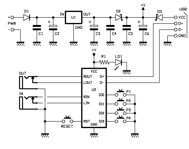
Moreover, and as shown by the circuit diagram, there are both the input and the output connectors for Line-In and Line-Out (and named IN and OUT), and 5 buttons, of which 4 can be programmed as required. Reset is dedicated to the reproducer’s hard-reset, while P1, P2, P3 and P4 can be programmed as desired, by interacting with the configuration file, as it will be explained in the next post. For a quick interaction we suggest to use the configuration file attached to the project, as it proves to be already adjusted to offer the following functionalities: serial communication in CLI mode, by means of USB connection and input functionality, as shown in Table. Morever, the file configures the dedicated I/Os as inputs, with an internal pull-up enabled, high idle condition and minimal duration of the low logical impulse at 700 ms.
| Input | Button | Command | Functionality |
| IO0 | P1 | 1 | It starts the execution of the files contained in the play list |
| IO1 | P2 | 2 | It stops the current execution |
| IO2 | P3 | 4 | It activates or deactivates the pause |
| IO3 | P4 | 5 | Avvia la registrazione nominando il file secondo i parametri di conf.ini |
Table 2. Description of the functionalities associated to the conf.ini sample file, for the usage of the buttons on the sample demoboard.
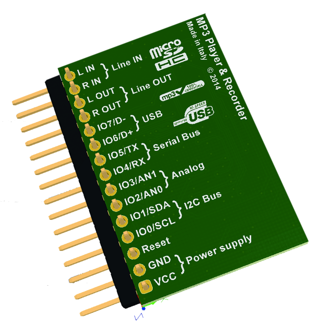
The pinout
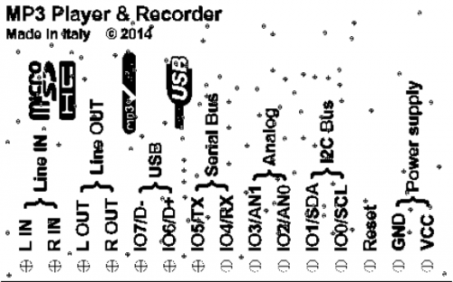
All the connections to be brought to the outside, for the interaction with a possible circuit with which to integrate the module (but also for the demoboard we will talk about in the next issue, on the occasion of the second episode) are on a 15 pins (single-in-line) angle header.
The lines’ layout is illustrated by the dedicated serigraphy on the back side of the circuit.
Going in order, let’s analyze each one of them, as follows. The first two pins are used to give power supply to the circuit. Pin 1 corresponds to positive power supply, and can be 5V or 3,3V; in any case the GPIO will always be at 3,3V and is not 5 V tolerant; thus in the case the circuit will have to interact with a 5V IO device, it will be needed to adapt the input signals to the player, so to avoid overvoltage at the said signals.
Pin 2 is a mass reference, be it for the power supply and for the Line-In and Line-Out analog signals. To avoid interferences coming from digital signals, we advice to use a very big GND line, so to reduce as much as possible the effect of voltage drops or due to the sharing of the same reference with digital and analog GNDs.
Pin 3 directly interacts with the U2 microcontroller reset, and in normal operating conditions it is enough to leave this input disconnected. To send a hard reset impulse it is enough to force this line at a low logical level for a few milliseconds. Once released, the line will return again to 3,3V, via R2. Pins number 4 and 5 are the first IO pair that can be programmed by the user, as desired. On these pins it is possible to enable the usage of the bus I²C (the player works as a slave unit), thus the pin functions respectively become SCL and SDA; for the proper operation of the bus it is needed to insert two pull-up resistors, as indicated by the specifications of the I²C protocol: in general a value between 2,2 kOhm and 10 kOhm is enough. By means of the I²C protocol it is possible to interact with the reproducer, by reading and writing the internal registries that are dedicated to the I²C operating.
Vice versa, the same pin pair may operate as a general purpose IO, and they are respectively identified with GPIO0 and GPIO1: in this case it is possible to associate to each one of them an input function, or an output function, as shown in Table 5.
The second pin pair regards numbers 6 and 7, and to these pins the analog input function (not yet implemented in the software, v0.1) is dedicated. They are respectively identified with AN0 and AN1 or, as an alternative, they serve the general purpose IO function with the GPIO2 and GPIO3 nomenclature.
The next pin pair regards number 8 and 9, and to these pins a native UART peripheral is associated, respectively with the serial signals on RX and TX. When turning on (it is possible to disable the default functionality) the microcontroller will send log messages and will be tuning in, waiting for the commands given by the user. By disabling the serial functionality, it is possible to use these pins as a third general purpose I/O pair (GPIO4 and GPIO5).
Finally, the last programmable pin pair regards numbers 10 and 11, to which the D+ and D- functionalities of the USB bus are associated.
When the circuit is connected to a computer, the software simultaneously create a Mass Storage peripheral, allowing to explore the content of the microSD; and a Serial Port Emulator, that can be used to interact with the device in place of the native UART. If the USB Composite device Windows driver isn’t normally made available by means of the Windows driver recovery system, it is possible to add it manually: the driver can be found along with the project source. In the case in which the USB functionality is not a desired one, it is possible to configure the software so to use the general purpose IO with the GPIO6 and GPIO7 names, respectively. In the paragraph concerning the general purpose IO, we will explain how to associate a funtionality in Table 5 to one of the eight GPIO pins.
By continuing with the description of the functionalities associated with the connector, we find the pins 12 and 13, operating as a Line-Out; and pins 14 and 15, operating as a Line-In, compatibly with the standard levels, that are: Consumer audio at −10 dBV (Nominal level: 0.316 VRMS) as regards the audio signals.
| # | Name | Main Description | Alternative Description |
| 1 | Vdd | Power Supply, 5 V o 3,3 V. The GPIO is always at 3,3 V | |
| 2 | Gnd | Mass Reference | |
| 3 | MCLR | Hard reset | |
| 4 | SCL/IO0 | I²C clock | General purpose I/O number 0 |
| 5 | SDA/IO1 | Given I²C | General purpose I/O number 1 |
| 6 | AN0/IO2 | Analog Input number 0 | General purpose I/O number 2 |
| 7 | AN1/IO3 | Analog Input number 1 | General purpose I/O number 3 |
| 8 | RX/IO4 | UART native receiver | General purpose I/O number 4 |
| 9 | TX/IO5 | UART native transmitter | General purpose I/O number 5 |
| 10 | USB_P/IO6 | USB Data + | General purpose I/O number 6 |
| 11 | USN_N/IO7 | USB Data – | General purpose I/O number 7 |
| 12 | Rout | Line-Out, right output channel | |
| 13 | Lout | Line-Out, left output channel | |
| 14 | Rin | Line-In, right input channel | |
| 15 | Lin | Line-In, left input channel |
Table 1 – Description of the 15 pins angle header, pin spacing 2.54mm.
From the Store
