Introduction
The imminent large-scale rollout of 5G technology imposes new and tough challenges for designers of PCB, network equipment and electronic devices in general. 5G will not only represent an increase in data rates, but it will be a real revolution, with latency times reduced up to 1ms and the use of millimeter waves (mmWave) to support greater bandwidth. PCBs for 5G mobile and network devices must be able to simultaneously manage higher digital data rates and higher frequencies, pushing mixed signal design to its limit. 5G applications will also pose a variety of new challenges for the engineers developing automated test equipment (ATE). Compared to the current 4G mobile network, the rollout of 5G will force designers to rethink the layout of PCBs used in mobile devices, data transmission networks and IoT infrastructure. Ensuring signal integrity at every point on the board represents one of the most difficult challenges imposed by 5G testing. Due to the presence of mixed signals, it will be necessary to prevent EMI between the analog and digital sections of the board, verifying that the FCC EMC requirements are met.
Impact of 5G features on testing
Transition from 4G to 5G network will not only result in a substantial improvement in data transmission rates and greater bandwidth availability but will also introduce new features that are destined to radically change many aspects of our lives. 5G network aims to provide 10-20x faster data rates (up to 1 Gbps), an increase in traffic of up to 1000x and an increase of up to 10x in the number of connections per square kilometer. Latency will be very low, of the order of 1ms, about ten times lower than that obtainable with a 4G network. Low latency is essential for the implementation of applications with real-time behavior, such as virtual reality and augmented reality (VR/AR), machine-to-machine (M2M) communication systems and autonomous vehicle infrastructure sensors.
5G networks will operate on a much wider frequency range than was available with previous mobile technologies. Printed circuits intended for mobile devices and network equipment will have to simultaneously manage high speed digital signals and high frequency RF signals, pushing mixed signal design to its limits. While 4G network uses frequencies between 600 MHz and 5.925 GHz, 5G network will significantly expand its upper frequency limit, pushing itself into the millimeter wave (mmWave) band. Bandwidth per channel is also an important factor affecting the design and testing of 5G PCBs and devices. While in 4G network the bandwidth per channel was equal to 20 MHz (limited to 200 kHz in IoT devices), in the fifth generation mobile network we will have a bandwidth per channel equal to 100 MHz for frequencies below 6 GHz and 400 MHz for frequencies above 6 GHz.
PCBs designed for 5G applications will require analog and digital components capable of operating at very high frequencies and data rates, whose reliability and efficiency can only be guaranteed through effective thermal management. Temperature monitoring is therefore another relevant factor for assessing a correct behavior of the PCB or device.
5G device testing
The performance requirements imposed by 5G technology will create unprecedented challenges in the testing of integrated circuits, System-On-Chip (SoC), PCBs, mobile devices and network equipment. Most 5G NR (New Radio) installations will use the 3.5 GHz frequency and the 28 GHz to 29 GHz frequency range. Both of these frequency ranges are new to the cellular network and will require architectural changes and modifications to radio access techniques. The ability to achieve greater network capacity and higher transmission data rates will require the use of advanced technologies, such as massive MIMO (multiple-input/multiple-output) and beamforming.
While still in the early stages of deployment, 5G technology is gaining momentum, posing urgent questions about how and at what cost to test mmWave devices used in different RF front-end module architectures and networking equipment. In addition, mmWave signals essentially propagate in the line-of-sight direction and are more subject to atmospheric attenuation than sub-6 GHz bands, resulting in the need to perform accurate tests capable of covering all operational scenarios. Phased array antennas, required to support advanced features such as beamforming, will benefit from the small size to allow for multiple antenna elements on the same PCB. The main challenge will be to reduce parasitics between the antenna and the low noise amplifier (LNA) on the receiving side, and with the power amplifier on the transmitting side. The fulfillment of the requirements must also be tested on the antenna, also using OTA (Over-The-Air) techniques. The use of millimeter waves will create new challenges for test systems. First of all, it will be necessary to reduce the distance that separates the test hardware and the cooling system from the probe environment, in order to minimize the particularly high-power losses created at mmWave frequencies. Additionally, testing boards and modules with integrated antenna will require a different approach, bearing in mind that in some cases only over-the-air communication between the test system and the DUT will be possible.
ATE tools
The complexity of the required compliance testing is growing exponentially with each new generation of mobile technology. Release 14 of 3GPP (which already contained some pre-5G functionality) specified about 15,000 tests, Release 15 (partial 5G) about 300,000 tests, whereas Release 16 (full 5G) will introduce additional tests. As the number of required tests goes up, the need for automated test systems increases, capable of supporting high frequencies and speeds and easily configurable. Automated Test Equipment (ATEs) are essential to ensure the proper functioning of PCBs, SoCs or individual components used in the implementation of the 5G network.
ElevATE Semiconductor is a leading company which provides world class test integrated circuits (ICs) that address the industry’s most complex ATE challenges. Designing state of the art chips, ElevATE delivers the highest density, lowest power ATE solutions available. ElevATE products can be grouped into four main categories, depending on the technology on which they are based:
- integrated pin electronics products – ElevATE is the market leader in low power, high density integrated pin electronics. Developed in a pure CMOS technology, these products enable customers to develop next generation high density instruments with increased parallelism fro reduced cost and improved system reliability;
- integrated DPS products – these Device Under Test (DUT) power supply solutions incorporate up to 8 independent DUT Power Supply Unit (DPS). The interface, the control, and the I/O are digital, while all analog circuitry is inside the chip. A single chip is able to provide a complete DPS solution;
- integrated PMU/VI products – Parametric Measurement Units and Virtual Instruments provide best in class density as high as 8 channels per chip and voltage up to 60V. PMI and VI products are cost-sensitive solutions that provide both voltage and current source and measurement capability for a wide range of applications;
- integrated high voltage products – based on a highly integrated dual channel wide voltage System-on-a-Chip (SoC) pin electronics solution, these products incorporate every analog function, along with some digital support functionality, required on a per channel basis for Automated Test Equipment.
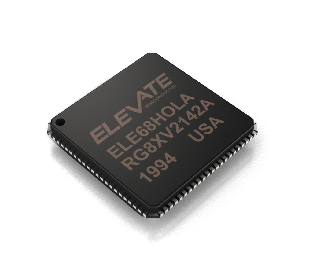
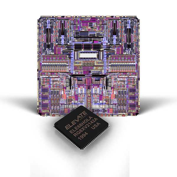
Among ElevATE portfolio solutions is the Venus 4 (ISL55161), a highly integrated SoC incorporating a dual channel 400MHz/800Mbps pin electronics differential driver and comparator, active load, timing deskew, PMU and DAC. Available in a 64-Lead 10mm x 10mm TQFP and in a 64-Lead 9mmx9mm QFN package, the SoC features a Pdq ≤ 500mW/Channel @ 11V Operation.

Figure 1: Venus 4 (ISL55161)
The SoC, whose block diagram is shown in Figure 2, is particularly suitable for applications such as Automated Test Equipment (ATE), instrumentation and ASIC verifiers.

Figure 2: Venus 4 block diagram


The high data rates and processing power required for 5G can generate significant heat in devices, which can affect performance and reliability. Thermal test systems are used to measure and manage the heat generated by 5G devices during operation.