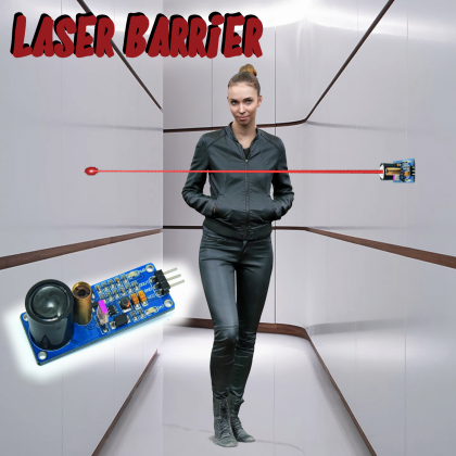
It allows us to detect the presence and passage of an object thanks to the combination of a laser diode which emits a light ray and a phototransistor which detects reflected light.
Robotics applications and industrial control systems normally make use of optical systems in order to detect proximity and passing of objects, taking advantage of light interruption or light reflection on a surface of the object to be detected. In this article, we want to show you the project of a laser barrier: however this is not an interruption-type barrier, which needs the object to be detected to pass through a meter and a photodetector, in fact, this is a reflection barrier: in our circuit, a laser projects a ray of focused and infinitely-collimated light and any object passing in front of it will reflect a portion of it, which will be intercepted by a lens on its way back and focused on the sensible surface of a photo-sensible component. In this barrier, therefore, the object to be detected doesn’t have to interrupt a ray of light but direct it towards a photodetector. One advantage of this type of device is that it doesn’t require the placing of a sensor at a distance, with the inevitable wiring required, in fact, it concentrates all the electronics needed in just one place and therefore it is ideal for mobile systems like wheeled robots or robots on tracks. Typical detection distance is 80 cm but he can reach a maximum of 1.5 m; everything depends on how dark and absorbent the object is, in other words, how much light does its surface reflects. The circuit, thanks to its nature, can be used in order to detect obstacles, as a unit counter on a conveyor belt, counter for people passing through a gate etc.
Circuit diagram
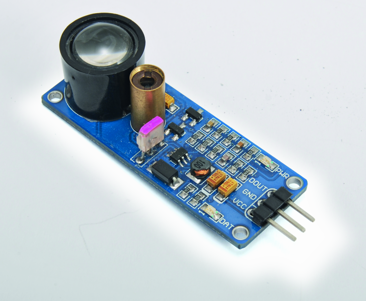
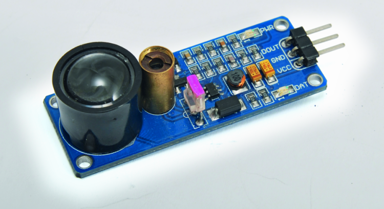
So, let’s take a look at the circuit, where we can see that it employs a laser as the transmitter and a phototransistor-based module (labeled H2) as the receiver. The beam emitted by the transmitter is reflected on the surface in front of it and it hits the lens (its purpose is to focus the reflected light on the phototransistor) of the emitted by the LASER and avoids disturbances from other light sources.
Laser diode is a small pointer (which is a component integrating a laser diode which is cooled by the dedicated casing, a voltage regulator, and a collimator lens) and it is labeled LASER in the diagram and is powered through the Q1 transistor (a BC817 mounted in common emitter configuration) which base is piloted by the 180 kHz rectangular signal locally produced by an oscillator; this is labeled H1 on the circuit diagram. For every high logic level coming to the 1-pin of the oscillator (2-pin being the 5 V power source of the oscillator module), the transistor goes in saturation and powers the laser diode, which emits a light impulse; during the process, the transistor is in interdiction and the laser diode is turned off. When on, its current is limited by Q1’s collector resistance (R5).
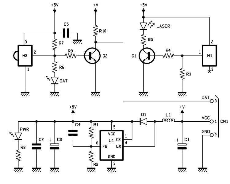
The light impulses are sent out frontally and when they hit an object with a surface capable of reflecting at least part of them, they come back to the circuit, where part of them hit the phototransistor’s lens that conveys them on the exposed junction; if the portion of reflected laser light reaching the phototransistor is sufficiently intense, the junction shows free charges (we are talking about electrodes, because transistor is an NPN, although for every electron moving out you also get an electron hole…) forming the base current, which is then amplified by the collector’s electric field, thanks to the 5 V power reaching the phototransistor’s collector from the 3-pin (ground – 1-pin – relates to the emitter’s resistance). The phototransistor makes the signal of its emitter available on 2-pin and the signal is sensible to infrared and visible light; it is in common collector configuration, so its collector is powered through contact 1 and contact 2 provides around zero volts with no light and about 4 V on the base when receiving light.
Q2 transistor, which is a BC817 also mounted in common collector configuration, is in saturation when on standby due to the pull-up resistor R7, which polarizes its base through R9; the condition is highlighted by the lighting of LED labeled DAT, which current is limited by R6 resistance. When the phototransistor is hit by a light of sufficient intensity, its collector drops from 5 V to a little less than 0.7 V, such voltage is not enough to keep the polarization of Q2’s base, which goes now in interdiction and its collector switches to high logic level. This line can be read by a microcontroller in order to detect the presence of an object; high logic level is 5 V and the low logic level is around 0 V, so the line can interface with logic systems operating at TTL levels. The DAT LED repeats the output status of the same name and inverts it, in fact when this one is on due to the phototransistor receiving light on its base (which means an object is present), the output is at low-level, while when there is no light detected, it turns off and DAT output goes to logic level 1.

Note that the choice to pilot the laser diode with a rectangular-shaped wave instead of a continuous signal comes from the necessity to make the sensor immune to lights and environmental disturbances, in fact, if the laser was constantly on, DAT would have (in case of light coming on the phototransistor right after the reflected) a voltage which may be influenced by environmental light, since the phototransistor could be constantly conducting if sufficiently lighted or hit by other light radiations falling within its sensibility spectrum. On the other hand, if we emit light impulses of a certain frequency we can use a receiver module with filter and have it receiving only those impulses, discarding continues light components. In fact, the H2 has an 180 kHz signal filter on its output (2-pin) which allows only signals produced by laser impulses pass.
The use of a bandpass filter on the circuit output discriminates signals, eliminating possible light impulses external to the detection system based on our circuit; besides, it relieves the possible microcontroller interfaced with DAT contact of such duty. Note that the high on-off frequency of the laser does not interfere with the detection since the impulses, although short, are infinitely longer than the short delay introduced by the reflected light hitting the phototransistor. The entire circuit is powered by a somewhat flexible voltage that can range from 2.5 V to 12 V thanks to an integrated switching regulator (labeled U1) which keeps its output to 5 V regardless of load conditions and the voltage on Vcc input compared to ground. Power voltage is filtered locally by the electrolytic capacitor C1. Switching is based on a PT301 integrated circuit, which is a high-efficiency step-up DC/DC compact, equipped with PWM Adaptive Current Mode regulation. Inside it we can find an error amplifier, a ramp generator and a voltage comparator to implement PWM modulation (it compares the ramp signal with the continuous component relegated on the FB pin by the resistive divider R1/R2 and filtered by the capacitor parallel to R1) in addition to a N-channel enhancement-mode MOSFET to pulse on the inductance and to extract PWM’s impulses and its respective driver stage. The internal MOSFET can commute currents up to 300 mA, so if you need to handle higher currents, you can use the auxiliary output (EXT pin) to pilot a higher powered external MOSFET; in this case the output corresponding to the internal MOSFET ‘s drain (LX pin) goes parallel to the external MOSFET’s. The particular thing about the integrated is that it can start up and function with voltages less than 1 V (0.8 V being the minimum) at its input, this makes it ideal for battery-powered applications; the integrated can provide 3.3 V and 100 mA when powered by an alkaline 1.5 V battery and 5 V with 300 mA when powered by a Li-ion cell (1s) or Lipo cell (3,7V). The extremely high efficiency (over 90%) is also guaranteed by the low ON-resistance of the MOSFET and the high commutation frequency of 500 kHz allows to scale down commutation and filter components, that is the L1 inductor and the C3 capacitor (C4 too actually, which is a residual filter at 500 kHz).
This switching functioning is as follows: after the start, through L1 inductance and D1 diode, the integrated receives current (5-pin, Vcc); C3 and C4 start to charge up and, right after that, the integrated starts functioning and its internal circuitry (i.e. the comparator) sends a positive impulse on the MOSFET’s gate causing a short-circuit (ON status) between its drain and its source and therefore all the current flows towards ground; during this interval, the integrated is powered by the voltage coming from C3 and C4.
In the meantime, the inductor charges up and right after that the MOSFET goes into interdiction, then the energy stored in L1 is discharged (since the inductance does not keep it but tends to keep the current right before MOSFET’s interdiction, thus generating an inverted extra voltage with positive polarity on the diode’ anode) through D1 diode, from which it passes on to Vcc, C3 and C4, then to the output of the DC/DC converter to power the % V line (The LED connected in series to R8 resistance signals the presence of output tension of the converter).
Based on the tension coming back on FB pin, the comparator sets the width of the next voltage impulse to send to the MOSFET’s gate, which closes once again the coil in short-circuit for a period that is as longer as the voltage detected by FB is lower (and vice versa) thus charging the inductance again. The cycle starts over as described and goes on till power is cut off.
The integrated continues working once powered up because the CE pin is directly connected to Vcc; if we connect it to ground, on the other hand, everything goes in standby; in this condition, the converter is down and absorbs just 14 µA.
From openstore

[…] Build an open source Laser Reflection Barrier […]