[youtube id=”0721A1kZ3s0″ width=”620″ height=”360″]
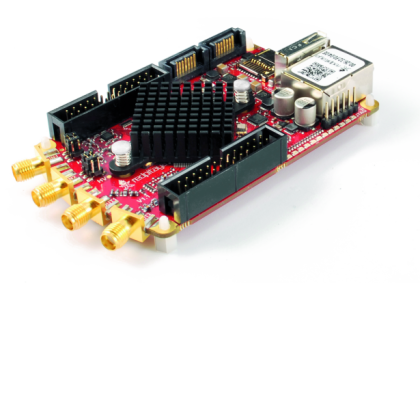
Here we present a tool to measure and acquire data. It is open source, and made by using the Xilinx Zynq 7010 Soc. It was funded with KickStarter and it is suited to be customized and adapted to various application exigencies.
The idea, which required funds for 50.000$ for its creation, obtained instead over 256.000 $ (in funds) from the supporters. What is it about? This time it is a real treat: a “virtual” tool to measure, acquire, elaborate and present data, a tool that can be customized and reconfigured, whose dimensions are those of a credit card. Its heart is a Zynq 7010 SoC, a sort of monster that groups (together) a FPGA platform and a Cortex A9 dual core processor inside, and by chance, it houses (on board) a GNU/Linux distribution for the complete management of the board. With Complete Management we mean that you just need to turn on the board and connect it to a network to have the preinstalled functions directly available on a web browser.
Xilinx Zynq-7010

The family of Zinq-7000 modules has been manufactured to combine the possibility of software programming, typical of a Processor for data processing, with the contemporary possibility of hardware programming, which is instead typical of FPGA platforms. This combination allows levels of performance, flexibility and scalability that we have never seen before. All of this is accompanied by lesser consumptions, lesser costs and reduced times for development and creation. With the SoC architecture of the Zynq-7000 family, it is possible to create solutions in which each component is optimized and located on the platform that may express its functionalities at best.
A module to acquire data or one for PID control as well as one for signals generation may profit the most from the features of the FPGA platform; while an application for communication or data presentation, e. g. via web, will be more properly created in the GNU/Linux environment of the elaboration processor. The processes running on the FPGA platform act independently from the processor hosting GNU/Linux. They will work even if this one last one is turned off. The development tools for both platforms are the standard development tools for each environment: HTML and C programming language for the GNU/Linux operative system, the standard development chain named “Zynq-7000 AP SoC Development Tools” for the FPGA. The SoC being the heart of the Red Pitaya is the Xilinx Zynq-7010, having the features listed:
| Zync 7010 | |
| Processor | ARM Cortex A9 dual Core |
| Coprocessor | NEON A chip with single and double precision in Floating point, for each processor |
| Level 1 Cache | 32 KB for the instructions and 32 KB for the data for each processor |
| Level 2 Cache | 512 KB |
| On-Chip Memory | 256 KB |
| Memory interfaces | DDR3, DDR3L, DDR2, LPDDR2, 2x Quad-SPI, NAND, NOR |
| Peripherals | 2x USB 2.0 (OTG), 2x Tri-mode Gigabit Ethernet, 2x SD/SDIO |
| FPGA Platform | Zync 7010 |
| Logic Cells | 28K Logic Cells |
| BlockRAM (Mb) | 240 KB |
| DSP Slices | 80 |
Setup
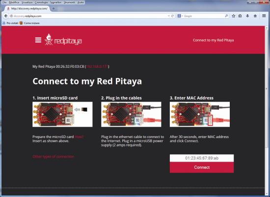
The compressed file used to set up the SDCard with the operative system and the FPGA image can be downloaded from the website https://www.dropbox.com/s/8z9tpgq88fm0zqw/redpitaya-SD-0.90-299-1278-apps-0.90-149-1278.zip. The operative system for the management of the ARM processor is a GNU/Linux distribution: this helps us to familiarize with the management of the small monster, at least in the beginning. Once the file is downloaded, we find two pleasant surprises. The first one concerns the limited dimensions of the file, a little bit more than 14 Mbs. It is nothing in comparison to downloads of 1 Gb and more that contain the “classic” images. The second surprise regards the FAT32 format of the SD Card, that makes it interoperable, or at least readable on other systems: as we already experimented with Arduino Yun. Given these features, to prepare the SD Card it is enough to decompress the file in a destination folder created for the purpose and to copy its content on the SD Card. It is also possible to decompress the file directly on the (same) SD Card. Once the software has been downloaded, we dismount the SD Card from the PC and put it into the predisposed slot on the Red Pitaya board. Let’s plug the Ethernet cable and power the board. We used a 5V power supply with a 2A micro USB plug that we usually choose when charging Raspberry Pi. As another pleasant surprise, we do not have to find out which IP address has been assigned to our board. The development community already thought about that. From a PC, let’s open a web browser and type in the address of the official website of Red Pitaya http://redpitaya.com/ in the URL bar. Here you may find characteristics, information and software to deepen your knowledge on the subject and update the software for the board. For the time being, let’s click up and to the right, on “Connect to my Red Pitaya” (http://discovery.redpitaya.com/), so to open the page as in figure.

Down and to the right in this page we may find a field where to type in our board’s MAC address (Media access Control). The MAC address is the univocal physical address assigned to any device suitable to be connected to a communication network. It is made by six bytes, the first three identify the manufacturer of the device, while the last three ones form the univocal identifying number assigned by those to each item. It is found on the label attached on the Ethernet connector. The code shows the hexadecimal sequence of six bytes divided by dashes, e.g.: 12-34-56-78-90-ab. We type it in the relevant field and click on the red “button” “Connect”.
After a short research we will be given the IP address assigned to Red Pitaya by our local network’s DHCP, as showed in figure. By clicking on the link we will be answered by the web server embedded in the board’s GNU/Linux section, with the page presenting the software preinstalled on the same.
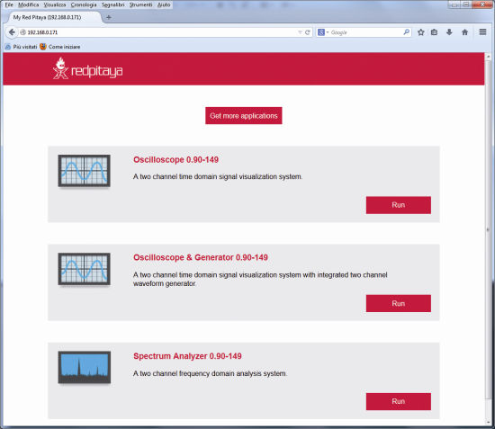
Here we find a tools panel, that alone may substitute many different expensive lab tools for measuring and controlling. It is definitely easy to activate, even for a non-specialist user, and especially if we think to comparable tools that are available on the market. For the time being, we shall stop the enthusiasm a bit, and start to analyze in depth this technology concentrate. Let’s start from what we can see. The heart of the board, that is the SoC Xilinx Zynq 7010, is placed under a generously big heat sink, to remind us that when FPGAs work, they do heat… a lot.
Hardware Overview
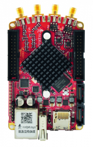
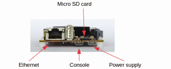
From the point of view of the physical layout, the board is around the size of a credit card. The big heat sink for the SoC stands out, with a crown of connectors all around. From a side of the board, apart from powering, we find the connectors depending mainly on the board’s ARM processor:
- A micro USB connector to power the board at 5V and 2A;
- A micro USB bringing externally the ARM processor’s console;
- A USB 2.0 standard connector to link external devices, as in a WiFi dongle;
- A slot for a micro SD Card, up to a capacity of 32 Gb;
- A RJ45 Ethernet Gigabit connector.
From the other side of the board one can see the four SMA connectors, forming two inputs and two RF outputs for the board. They are analog inputs and outputs with the following features.
Two input RF channels with the following features:
- Band width: 50 MHz (DC coupled, 3dB BW)
- Sampling frequency: 125 Msps
- ADC 14 bit resolution;
- Input impedance: 1 MOhm // 10pF
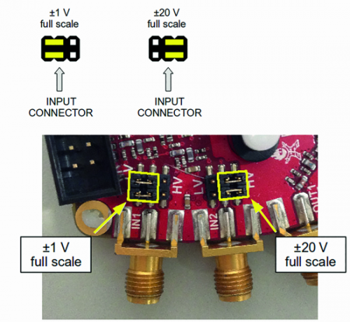
- Maximum input voltage: it can be configured through couples of jumpers placed at the spot of each connector, allowing to configure the maximum input voltage at +-1V or +-20V, as seen in figure. One has to pay attention so that, for each connector, both jumpers are placed on the same side, either on the LV or HV position. Different positions are not allowed;
- Overload Protection Diodes;
- SMA Connector.
Two output RF channels with the following features:
- Band Width: 49 MHz at 3dB (DC coupled, 3dB BW defined by anti-imaging filter)
- Sampling Frequency: 125 Msps
- DAC resolution: 14 bits
- Output Impedance: 50 Ohm
- Maximum power: 10 dBm on a load of 50 Ohm;
- Output slew rate: 200 V/us
- Short Circuit Protection;
- SMA Connector.
Let’s see now the LED sequence alongside of the Ethernet Connector. Some of these LEDs signal the board’s operating status while the other ones are available for the users and managed through a program. Table 1 summarizes the correspondences between LEDs and FPGA’s pins. Keep in mind that a bright green LED means that the board is correctly powered and the blue LED points the correct operating status of the FPGA. The yellow LED that you can see flashing, in the default distribution, is managed by the program.
| Table 1 LED Description |
||
| LED | FPGA Pin | FPGA Pin Description |
| Yellow 0 | F16 | IO_L6P_T0_35 |
| Yellow 1 | F17 | IO_L6N_T0_VREF_35 |
| Yellow 2 | G15 | IO_L19N_T3_VREF_35 |
| Yellow 3 | H15 | IO_L19P_T3_35 |
| Yellow 4 | K14 | IO_L20P_T3_AD6P_35 |
| Yellow 5 | G14 | IO_0_35 |
| Yellow 6 | J15 | IO_25_35 |
| Yellow 7 | J14 | IO_L20N_T3_AD6N_35 |
| Yellow 8 | E6 | PS_MIO0_500 |
| Red | D8 | PS_MIO7_500 |
| Green | K18 | |
| Blue | R11 | DONE_0 |
Let’s move to the two D-sub connectors on the long sides of the board. Even in this case we have another pleasant surprise. They are 2×16 pin connectors with a step of 2,54mm. They exactly reflect the GPIO connector of Raspberry Pi. Consequently, for our experiments we may use the connectors, flat cables, shields with terminals and link for matrix breadboards already available for sale for Raspberry PI. Clearly we cannot use the expansion shields because the meaning and management of the pins is completely different. But it is already very good like this. Let’s start from the E1 connector, the one placed on the side of the board with the LEDs. The main functions attested on the connector are the digital I/O (16 single-ended or eight differential) and corresponding powering. All the Pins work with a high logic level at 3,3 V. In Table 2 the meaning of the pins and the correspondence of each one with the pins of the FPGA platform is described.
| Table 2 E1Connector PinDescription |
|||
| Pin | Description | FPGA Pin | FPGA Pin Description |
| 1 | 3V3 | ||
| 2 | 3V3 | ||
| 3 | DIO0_P | G17 | IO_L16P_T2_35 |
| 4 | DIO0_N | G18 | IO_L16N_T2_35 |
| 5 | DIO1_P | H16 | IO_L13P_T2_MRCC_35 |
| 6 | DIO1_N | H17 | IO_L13N_T2_MRCC_35 |
| 7 | DIO2_P | J18 | IO_L14P_T2_AD4P_SRCC_35 |
| 8 | DIO2_N | H18 | IO_L14N_T2_AD4N_SRCC_35 |
| 9 | DIO3_P | K17 | IO_L12P_T1_MRCC_35 |
| 10 | DIO3_N | K18 | IO_L12N_T1_MRCC_35 |
| 11 | DIO4_P | L14 | IO_L22P_T3_AD7P_35 |
| 12 | DIO4_N | L15 | IO_L22N_T3_AD7N_35 |
| 13 | DIO5_P | L16 | IO_L11P_T1_SRCC_35 |
| 14 | DIO5_N | L17 | IO_L11N_T1_SRCC_35 |
| 15 | DIO6_P | K16 | IO_L24P_T3_AD15P_35 |
| 16 | DIO6_N | J16 | IO_L24N_T3_AD15N_35 |
| 17 | DIO7_P | M14 | IO_L23P_T3_35 |
| 18 | DIO7_N | M15 | IO_L23N_T3_35 |
| 19 | NC | ||
| 20 | NC | ||
| 21 | NC | ||
| 22 | NC | ||
| 23 | NC | ||
| 24 | NC | ||
| 25 | GND | ||
| 26 | GND |
From the opposite side of the board we find the E2 connector, reporting the pins of the serial communication buses, I2C and SPI. There are even four inputs (ADC) and four analog outputs (DAC) in addition to two external clocks for the analog RF inputs and to the 3,3V, 5V e GND powering. The analog input channels have the following features:
- Sampling Frequency: 100 ksps;
- ADC Resolution: 12 bits;
- Passband: 50 kHz.
The analog output channels have the following features:
- Type: PWM Low pass filtered
- PWM Modulation Frequency: 250 MHz
- Nominal Sampling Frequency: 100 ksps
- Equivalent PWM Resolution: 11.3 bit
Table 3 shows the meaning of the pins of the E2 connector and the correspondences with the pins of the FPGA platform.
| Table 3 E2connector pinDescription |
||||
| Pin | Description | Pin FPGA | FPGA Pin Description | Levels |
| 1 | +5V | |||
| 2 | -3V3 (50mA) | |||
| 3 | SPI(MOSI) | E9 | PS_MIO10_500 | 3.3V |
| 4 | SPI(MISO) | C6 | PS_MIO11_500 | 3.3V |
| 5 | SPI(SCK) | D9 | PS_MIO12_500 | 3.3V |
| 6 | SPI(CS#) | E8 | PS_MIO13_500 | 3.3V |
| 7 | UART(TX) | C8 | PS_MIO08 | 3.3V |
| 8 | UART(RX) | C5 | PS_MIO09 | 3.3V |
| 9 | I2C(SCL) | B9 | PS_MIO50_501 | 3.3V |
| 10 | I2C(SDA) | B13 | PS_MIO51_501 | 3.3V |
| 11 | Modo com. | GND (default) | ||
| 12 | GND | |||
| 13 | ADC 0 | 0-3.5V | ||
| 14 | ADC 1 | 0-3.5V | ||
| 15 | ADC 2 | 0-3.5V | ||
| 16 | ADC 3 | 0-3.5V | ||
| 17 | DAC 0 | 0-1.8V | ||
| 18 | DAC 1 | 0-1.8V | ||
| 19 | DAC 2 | 0-1.8V | ||
| 20 | DAC 3 | 0-1.8V | ||
| 21 | GND | |||
| 22 | GND | |||
| 23 | Ext Adc CLK+ | LVDS | ||
| 24 | Ext Adc CLK- | LVDS | ||
| 25 | GND | |||
| 26 | GND |
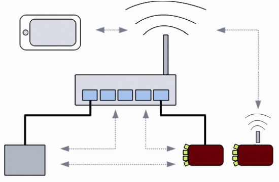
The two SATA connectors alongside of the SD Card housing give access to four couples of digital signals that allow synchronization and data transfer on daisy connections, up to a speed of 500 Mbps. We already saw, at the beginning of this article, how to turn on a Red pitaya board and access the available functionalities from a simple connection via web browser. Indeed, it is possible to connect to Red Pitaya in many other ways, via web or through remote terminal or serial console. Remaining in the Internet home network mode, we want to point out the different possibilities in addition to the Ethernet cable connection:
- Connection to the board from mobile devices, such as smartphones and tablets;
- Assignation of a static IP to the board;
- Connection of the board to the home network, in WiFi mode.
All of this is summarized in figure. As for the method to connect to the board via browser from mobile devices, it is exceedingly easy. You just need to connect and associate our device to the Access Point of the home network and follow the same procedure explained in the beginning of the article. If you already know the IP address of Red Pitaya you may type it directly in the URL bar of your browser.
On the other hand, if we wanted to assign a static IP to the board, we have to remember that a part of the heart of the board itself is managed by the GNU/Linux operating system, and that we therefore may use the classic tools that we already showed in the many articles dedicated to Raspberry Pi. The board’s operating system includes a SSH server already active when switching on the device. We may therefore connect ourselves in remote terminal mode with the tools we already know: PuTTY as a remote shell and WINScp as remote file manager. Let’s start up WINScp and connect ourselves to the Red Pitaya board as “root” user, the only user who is enabled by the board. By the way, the password is “root”. Once inside the file system, that mirrors a classic GNU/Linux file system, let’s go to the folder /etc/network and open the file “interfaces” by double clicking with the mouse.

We shall modify it as follows, and we’ll comment the lines with the character #:
iface eth0 inet dhcp
udhcpc_opts -t7 -T3
and uncomment the configuration contemplating the static IP. Of course the address configuration has to be coherent with the settings of your home network and the static address has not to be included in the range of addresses that are automatically assigned by the DHCP service.
# Red Pitaya network configuration
#
###########################
# lo: Loopback interface #
###########################
auto lo
iface lo inet loopback
######################################
# eth0: Wired Ethernet – 1000Base-T #
######################################
#
# Uncomment only one: dynamic or static configuration.
#
# Dynamic (DHCP) IP address
#iface eth0 inet dhcp
# udhcpc_opts -t7 -T3
# Static IP address
iface eth0 inet static
address 192.168.1.101
netmask 255.255.255.0
gateway 192.168.1.1
################################
# wlan0: Wireless USB adapter #
################################
auto wlan0
iface wlan0 inet dhcp
pre-up wpa_supplicant -B -D wext -i wlan0 -c /opt/etc/network/wpa_supplicant.conf
post-down killall -q wpa_supplicant
udhcpc_opts -t7 -T3
From the remote shell we give the “reboot” command and, after a while, we connect ourselves again to the board, with the new address. When switching on, we’ll see the blue and green leds turning on, and then we’ll see the yellow LED 0 starting to flash. Among the other connection possibilities, we shall keep in mind the direct connection to the board’s serial console, that allows to access directly the operating system’s shell. Let’s connect a cable with micro USB plug to the board’s micro USB port. We have to connect the other end of the cable to a USB connector of the PC. The board should be automatically recognized as a FTDI device and be assigned to a virtual COM port. The port number can be found by entering in the Control Panel>>System>>Peripherals Management>>COM ports. If this doesn’t happen and the connection to the device shows an error warning, with a small yellow icon, we have to manually install the driver for the management of virtual ports: we may download it at the address http://www.ftdichip.com/Drivers/VCP.htm. To connect ourselves to the serial console we shall always use PuTTy.
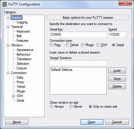
In Table 4 are listed the settings of the serial communication with the console.
| Table 4 Serial |
|
| Parameter | Value |
| Speed | 115200 |
| Data bit | 8 |
| Stop bit | 1 |
| Parity | None |
| Flow control | None |
When opening the serial window let’s press the “Enter” button a few times to “wake up” the console. We shall receive the shell prompt as a reply. From here we may type in all the commands allowed by the standard shell. We ifconfig typed the command, to “discover” the board’s address.
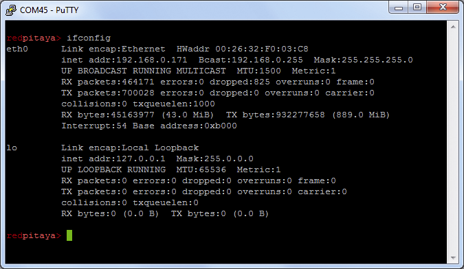
At this point we should have our board turned on and connected to the browser, set at the page of the available applications. Let’s click on the button “Get more applications”: it will send us to the “maintenance” page, concerning the environment and the available applications.
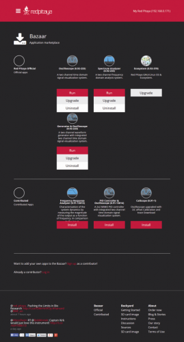
The place is named Bazaar, the marketplace of Red Pitaya applications. From here we may update the operating system by clicking on the “Upgrade” button in the ecosystem; or by installing, uninstalling and updating the available applications. Some applications are part of the “official” marketplace, some other ones are there as “contributions”. All of them are freely available and obviously one may contribute by making his own applications available. For instance, we added a frequency response analyzer to the basic applications.
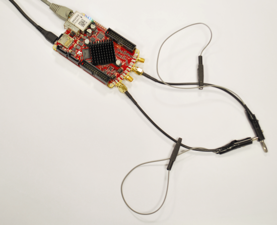
Let’s get back to the home page and do some tests. We shall loop a board RF output with a RF input. Let’s connect two cables to the board, one to the RF1 output and the other one to the RF1 input channel. We then connect the two cables, without connecting the mass terminals, as the channels’ masses are already connected. Given that the RF outputs allow a 50 Ohm load, for a well made connection we just have to load the output with a 50 Ohm load. Let’s link a SMA “T” Connector to to the RF output channel of the SMA connector. To one of the outputs that have remained free, we shall connect the “probe” cable, that we will then connect to the RF input. On the last “free” output, we shall then mount a “cap” with 50 Ohm impedance, that will be our load.
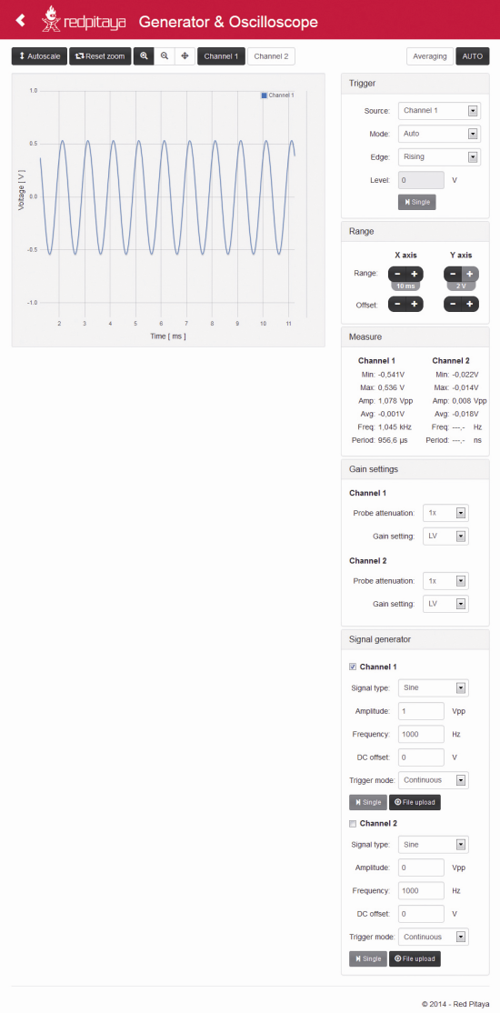
Let’s open the “Oscilloscope & Generator” application. This application allows us to generate a signal on the output channel and acquire it on the input channel, so to visualize it in the oscilloscope section of the application. In the meantime, we can see the main “commands” available on the application “panel”. In figure we can see the application panel with the numerical references for the various controls, the meaning of each one being described in Table 5.
| Table 5 Functions |
|
| Ref.Num. | Description |
| 1 | Autoscale: Sets up the voltage interval, so to represent at best, in the graphic visualization area, the input signal or the input signals. |
| 2 | Reset zoom: Brings back the setting of the temporal axis to the 0 – 130 µs range, and sets up the voltage interval to “full scale”. |
| 3 | Diagram tools: zoom in / zoom out / overview. |
| 4 | Channel enable buttons: Enables or disables the vision of the specific channel. |
| 5 | Averaging: Enables the calculation of the average of the samples during lengthy acquisitions. By setting the average of the values one can improve the signal/noise ratio, but in this way the information concerning possible high frequency peaks will be lost. |
| 6 | AUTO button: Sets up the optimal visualization mode for the signal being acquired. This functionality can be applied only to signals in the frequency range from 3 Hz to 50 MHz. |
| 7 | Trigger menu (click on the “Trigger” bar to expand the Trigger menu)
|
| 8 | “Range” Menu: The “Range” and “Offset” buttons allow to set up correctly the voltage interval, so to visualize correctly the signal’s track and to position it on the vertical axis, in the way you want. |
| 9 | “Measure” Menu: Acquires (statistical) values for voltage and frequency/time for both input signals. This functionality works correctly as regards to input signals having frequencies in the 3 Hz – 50 Mhz range. |
| 10 | “Gain settings” Menu:
|
| Signals Generation Section | |
| 1 | “Signal enable” Checkbox: Enables or disables the signals generator on a specific channel. |
| 2 | “Signal type”: Sets up the signal (wave) that has to be generated (sinusoidal, square, triangle wave, to be reproduced by sampling on file). |
| 3 | “Amplitude”: Sets up the width of the output signal. |
| 4 | “Frequency”: Sets up the frequency of the output signal. |
| 5 | “DC offset”: Sets up the output signal offset, that is to say, the deviation of the generated wavelength from the zero of the orizontal axis. |
| 6 | “Trigger mode”: Sets up the triggering signal modes (Continuous, Single, External)“Single” Button: By clicking on the “Single” Button, when the “Trigger Mode” is set up on “Single”, a single samples sequence lasting exactly as the preset frequency is generated (The last sample in the sequence is applied after the sequence is completed.) |
| 7 | “File upload”: Allows to load a file containing a sampling of the signal (in CSV format), that you want the generator to reproduce. |
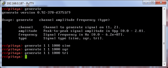
By operating on the “Signal Type” control we can modify the generated wavelength. We can also generate a signal starting from a sample that has been memorized on a file. The single applications, such as the oscilloscope and the signal generator, present the same controls of the joined application. Another interesting possibility is the generation and acquisition of signals from the command line in the system shell. To generate a signal one has to use the “generate” command.
Table 6 describes the parameters to customize the generated signal.
| Table 6 Parameters of Signal generator utility |
|||
| Name | Type | Range | Description |
| channel | int | 1 / 2 | Output channel selection |
| amplitude | float | 0 – 2 [V] | The maximum width of the signal able to be generated is 2V peak/peak. |
| freq | float | 0 –162000000 [Hz] | Frequency of the signal to be generated. Up to 62 Mhz for sinusoidal wave signals and up to 10 Mhz for square and triangle wave signals. |
| <type> | string | sine / sqr / tri | Waveform (Optional): (sine – sinusoidal wave signal , sqr – square wave, tri – triangle wave). If omitted, a sinusoidal wave signal is generated. |
Let’s open the oscilloscope application and generate a signal from the command, with a frequency of 1000 Hz, so to visualize it on the oscilloscope.
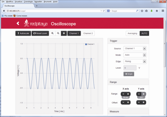
We shall now repeat the command, modifying the waveform and visualizing the results, as always on the oscilloscope. We shall use the same signal generation method to experiment with the spectrum analyzer. Let’s close the oscilloscope application by clicking on the icon with the “<” sign, so to return to the applications page, and let’s open the “spectrum analyzer” tool. Let’s generate a 1000 Hz tone with a sinusoidal wavelength: the result will be seen on the spectrum analyzer. We notice a vertical height marker that is much more extended as regards the width of the background noises, telling us that the noise signal of the generator is more than good, at least at 1000 Hz. We take the opportunity to introduce in the Table the description of the controls on the panel of the spectrum analyzer.
| Table 6 Functions of Spectrum analyzer |
|
| Annotation number | Description |
| 1 | “Autoscale”: Sets up the scale factor of the Y axis so to optimize the representation of the specter within the visualization area. |
| 2 | “Reset zoom”: It displays the whole frequency range and sets the Y axis to the range from -120 dBm to 20 dBm. |
| 3 | Visualization tools: zoom in / zoom out / overview. |
| 4 | “Channel enable” Buttons: Enable or disable the channel visualization. |
| 5 | “Channel freeze” Buttons: “Fix” the current representation of the specter for the desired channel. |
| 6 | Main Visualization Area. |
| 7 | Waterfall diagram for channel 1. |
| 8 | Waterfall diagram for channel 2. |
| 9 | Frequency range selection: The main frequency range covers DC to 62.5 MHz. Additional frequency ranges starting from DC are available in order to observe signal behavior at lower frequencies. For details concerning the frequency range check the specification document. |
| 10 | Peak Ch1: Shows the numerical value of the peak width for channel 1. |
| 11 | Peak Ch2: Shows the numerical value of the peak width for channel 2. |
Let’s try now to acquire a signal from command line, as always with the generator working.
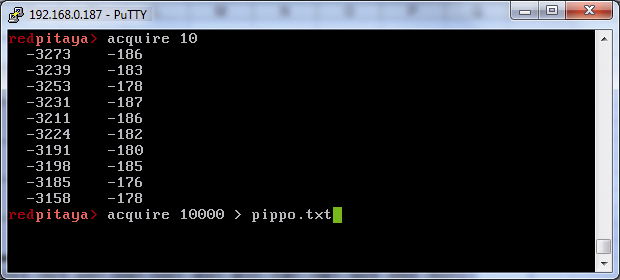
Figure shows the result of the acquisition directly “printed” to console. The second command generates a file with 10000 samples. We exported the file on PC by using WINScp and then imported it in a file into Excel. We then used the samples to generate a single line graph.

Always with regard to the command line, we’re gonna introduce the “monitor” command, that allows us to acquire a snapshot of the required values, depending on the parameters set.
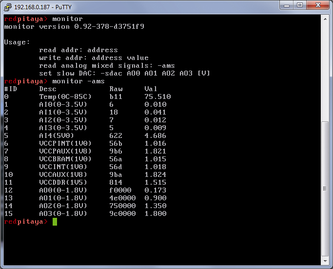
Here we asked for a list of the values of the analog inputs. One of them is assigned to measure SoC’s temperature. We said that in the beginning that FPGAs do heat. We shouldn’t have problems up to a temperature of 85°, but we’re getting close to it. We prefer, therefore, to mount a cooling fan over the heat sink: we stop ourselves here. There is still much to investigate about this product, as the possibility to access to single locations of the FPGA, the chance to write programs and applications on the GNU/Linux side and even to publish them in the Bazaar. Lastly, the chance to program the FPGA directly, with a free development environment.
We are studying… and we hope you do as well.

[…] It’s just that these Gifs are astoundingly elegant. 1) This is a a Reuleaux Triangle (There are curves of constant width besides circles and spheres. It’s a convex planar shape whose width is the same regardless of the orientation of the curve) 2) And these Curves of Constant Width can drill square holes. Red Pitaya: the opensource electronic laboratory. […]
An open source wifi module with UART/SPI/GPIOs/PWM for intelligent control,but fingertip-sized only
http://igg.me/at/xwifi/x
If this really was an open hardware platform, why do some people feel the need to reverse-engineer the schematics/PCB-layout of the pitaya?
http://www.eevblog.com/forum/microcontrollers/red-pitaya-hd-images-for-getting-the-schematic/
Stop writing lies that Red Pitaya is open source. There are not even full schematics of this board.