- Building a 3D Digital Clock with ArduinoPosted 3 months ago
- Creating a controller for Minecraft with realistic body movements using ArduinoPosted 4 months ago
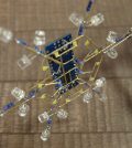
- Snowflake with ArduinoPosted 4 months ago
- Holographic Christmas TreePosted 4 months ago
- Segstick: Build Your Own Self-Balancing Vehicle in Just 2 Days with ArduinoPosted 5 months ago
- ZSWatch: An Open-Source Smartwatch Project Based on the Zephyr Operating SystemPosted 6 months ago
- What is IoT and which devices to usePosted 6 months ago
- Maker Faire Rome Unveils Thrilling “Padel Smash Future” Pavilion for Sports EnthusiastsPosted 6 months ago
- Make your curtains smartPosted 7 months ago
- Configuring an ESP8266 for Battery PowerPosted 7 months ago
Stack based solutions for image processing at the Edge and Cloud – Nick Ni & Adam Taylor
One of the beauties of image processing is its wide range of end applications from autonomous drones and cars, to medical and scientific imaging. This diverse range of applications brings with it a diverse range of requirements and solutions, from embedding the intelligence at the edge, to leveraging the power of the cloud. In either case, for their image processing system, users will face several challenges. This article looks at what these challenges are and how they can be addressed using an acceleration stack based approach.

 Figures 1 and 2 – Diverse examples Cloud based Medical Imaging and Edge based Agricultural Drone
Challenges
Applications processing at both the Edge and Cloud initially face a common problem, which is the implementation of the image processing algorithm such that it meets its overall system requirements. There will, in most cases, be a difference as to what that driving overall system requirement is. For an edge based implementation it may be the latency of the algorithm as the system may be required to make decisions based on information contained within. While a cloud based image processing solution may be driven by the requirement for exceptional accuracy as scientific or medical decisions may be based upon this.
Both implementations will also heavily rely upon deep machine learning and artificial intelligence, although in different manners. Edge based processing will use the classifiers generated by deep machine learning within the cloud to implement its object detection algorithms. While cloud based solution will use deep machine learning and Neural Networks to both generate the classifiers and then use these classifiers within its application.
It can be seen then, that both implementations require the capability to work with modern frameworks such as OpenCV, OpenVX, Caffe and FFmpeg to achieve their image processing requirement. But what about other requirements which dominate in these different implementations, these requirements must also be considered and addressed.
Processing within the Edge brings with it not only the need for real time processing and decision making but also its applications are often autonomous which brings other challenges. Autonomous operation brings a need for both a secure system and secure communications channels (when available) back to its operations centre. Autonomous systems are also often battery powered as such power efficiency is also a driving requirement. This leads to a tightly integrated solution which, along with implementing the image processing algorithm, is also capable of communicating with other sub systems or even controlling them. This is especially the case for drones where Size, Weight and Power (SWaP) constraints often combine the image processing system with other functions such as motor control, to create an optimal solution.
Implementing the processing algorithms within the cloud creates a different series of challenges, it is within the cloud that compute intensive algorithms are implemented such as deep machine learning, data analytics and image processing. These algorithms also face bottle necks in memory, storage and connectivity within the data centre limiting performance. While the applications implemented on the cloud may not be real time, often they require the ability to stream processed data in near real time and without drop outs to the client. This is the case in medical and scientific imaging which needs to be able to distribute a single image to several clients, this cannot be limited by bottlenecks in the system.
Stack Based Solution
Increasingly programmable logic in the form of All Programmable FPGA and System on Chip is being used to address these challenges. However, to fully leverage the capabilities provided by programmable logic we need not only the device but also an ecosystem which enables development using current industry standard frameworks and libraries.
This is where the Reconfigurable Acceleration Stack (RAS) and the reVISION™ stack from Xilinx come into play, designed to provide acceleration at the Cloud and Edge respectively. Both stacks are heavily based around the new paradigm of developing programmable logic using High Level Synthesis (HLS) which allows development in C / C++ / OpenCL and System C. Combining this HLS capability with library support for industry standard frame works and libraries such as OpenCV, OpenVX, Caffe, FFmpeg and SQL enables the necessary ecosystem to be established.
Both RAS and reVISION stacks are organized in three distinct layers very similar to the OSI seven-layer model which many engineers are familiar with. The lowest layer of the stack is the platform layer and it is common to both the RAS and reVISION stack. This is the actual hardware platform which contains the selected FPGA or SoC upon which the remainder of the stack is to be implemented, although the actual underlying technology is different for both stacks. When developing using reVISION the target device comes from either the All Programmable Zynq®-7000 SoC or Zynq® UltraScale™+ MPSoC system on chip families. While the RAS platform is based upon the use of All Programmable UltraScale™+ FPGAs, as such there is a difference in the remaining two levels of the stacks.
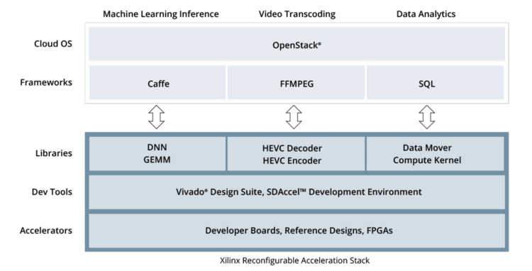
Figure 3 – Reconfigurable Acceleration Stack
When users are developing using the reVISION stack, the second layer is referred to as the algorithm layer and it is at this level they utilize the SDSoC™ design tool combined with commonly used open source libraries like OpenCV, to implement the algorithms required. Using SDSoC, they can partition the functionality between the processor system and the programmable logic of the chosen device to obtain the optimal system performance. While the final level of the reVISION Stack is the application layer which again uses industry standard frame works to create the overall application required for the solution.
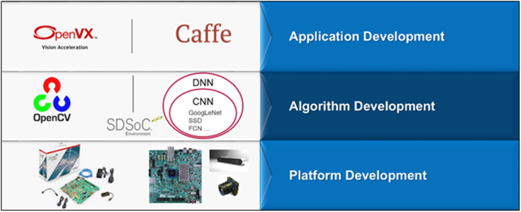
Figure 4 -reVISION Stack
The second level of the RAS is the application layer, this uses the SDAccel™ tool which again leverages HLS to implement its application with support for machine learning frameworks such as Caffe, integration with SQL environments and support for MPEG processing using FFmpeg. Of course, the same OpenCV libraries and frameworks as used within the reVISION stack can also be used at this level if required. The final level allows for integration within the data centre and is the provisioning layer, this uses OpenStack to provide the integration required.
Implementing these stacks within their solutions can bring about several advantages, many of which will be obvious, along with several which might not be obvious at first inspection.
Benefits of the Stack
The most obvious benefit which comes with the implementation of both stacks is the performance increase, which is achieved by executing image processing algorithms within the programmable logic. Compared to implementing the same function within a processor based architecture, RAS provides a 40 times improvement when implementing image processing algorithms and 11 times when performing deep machine learning. While using the reVISION stack provides between 40 and 400 times acceleration depending upon the algorithm and SoC selected.
These significant performance improvements provided by RAS within the cloud enable not only a reduced hardware requirement to achieve the same performance, but also provide for a lower cost of ownership and operation as the power consumption is also significantly reduced. The cloud can also take advantage of the reconfigurable nature of FPGA’s at run time and re configure the programmable logic for different algorithms as they are called to be executed.
Using the reVISION stack at the edge not only do they obtain the same performance increase but again they are also able to leverage the any to any interfacing capability provided by the programmable logic. This is especially important in edge based solutions where they must interface with several different types of sensors which use both standard and bespoke interfaces.
Users also benefit from the most efficient processing power per watt, where these applications are often battery powered this enables the application to last longer on its batteries and hence achieve more. They can also leverage the power management features of the all programmable system on chip devices to scale the power consumption in line with the demands of the operating conditions, for example, detecting that a smart augmented reality headset is no longer being worn and entering a sleep mode to conserve battery life.
Both All Programmable SoC and FPGA also provide inherent security features such as secure configuration and the ability to monitor internal voltages and temperatures to detect unauthorized access attempts to the device.
Finally, they must also consider the future upgrade path and the need to support new standards, frameworks and interfaces as these are released. The use of programmable logic provides for a product technology roadmap which can easily scale due to its any to any interfacing capability.
Conclusion
As demonstrated, image processing is ubiquitous with applications both at the edge and the cloud, facing many of the same challenges. The use of acceleration stack based approaches which support development of image processing systems in both applications enables the system developer to leverage both the system and performance benefits which come with the use of programmable logic.
Both stacks presented are also very flexible and will be developed over time to add support for new frameworks and standards as they are introduced.
For more information, please visit this site.

Related Posts


-
 Arduino ISP (In System Programming) and stand-alone circuits
We use an Arduino to program other ATmega without...
- Posted 12 years ago
-
-
-
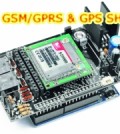 GSM GPS shield for Arduino
Shield for Arduino designed and based on the module...
- Posted 12 years ago
-
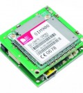
 Small Breakout for SIM900 GSM Module
Some post ago we presented a PCB to mount...
- Posted 13 years ago
-
 Building a 3D Digital Clock with Arduino
Project to create a digital clock consisting...
- Posted 3 months ago
-
 Acoustic amplifier – in DIY Kit
This kit creates a microphone amplifier with an output...
- Posted 4 months ago
-
 Creating a controller for Minecraft with realistic body movements using Arduino
Project of a controller that maps body movements...
- Posted 4 months ago
-
-
 Holographic Christmas Tree
Beautiful project to create a Persistence of Vision...
- Posted 4 months ago